We know that in the active region, the emitter–base junction is forward-biased and the collector–base junction is reverse-biased. Figure below shows the operation of a transistor with the emitter–base junction forward-biased and collector–base junction as open circuit. In this condition the normal PN junction diode action takes place.
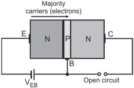
Forward-biased emitter–base junction with collector-base junction as open circuit
The width of the depletion region decreases due to the applied bias and there is a heavy flow of electrons from the N-type emitter to the P-type base. As the base is lightly doped compared to the emitter region, the width of the depletion region is larger in the base region as compared to that in the emitter region and a very small hole current flows from the P-type base to the N-type emitter region.
Figure below shows the structure of the transistor, when the collector–base junction is reverse-biased with the emitter–base junction open. In this condition, the transistor behaves like a normal reverse-biased junction diode. The depletion width increases with the increase in the reverse-bias voltage and is larger in the base region than that in the collector region. There is a small current flow due to the minority carriers (flow of electrons from the base region to the emitter region and flow of holes from the emitter to the base).
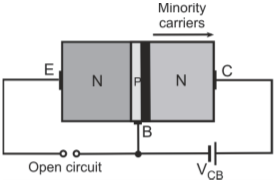
Reverse-biased collector–base junction with the emitter-bas junction open
When both the forward and the reverse voltages are applied simultaneously to the emitter–base and the collector–base junctions of an NPN transistor, respectively, it results in the flow of current as shown in the figure below.
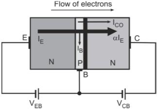
Flow of current in an NPN transistor in the active region
The emitter current (IE) consists of electron current (due to flow of electrons from emitter to base) and hole current (due to the flow of holes from base to emitter). The magnitude of hole current is negligible as compared to electron current, as the base is very lightly doped as compared to the emitter. Also, not all the electrons crossing the emitter–base junction reach the base–collector junction as some of them remain in the base region and constitute the base current (IB). Only a very few electrons remain in the base region as it is very thin and has low level of conductivity. The remaining electrons diffuse into the reverse-biased base–collector junction and travel across the base–collector junction easily as they are minority carriers in the P-type base region of the base–collector junction. This is referred to as the injection of the minority carriers into the P-type base region. These electrons diffuse across the reverse-biased junction to reach the N-type collector and constitute the collector current (IC). The magnitude of the base current is of the order of few microamperes and collector and the emitter currents are in the range of several milliamperes.
The emitter current (IE) can be expressed as sum of collector current (IC) and base current (IB). Therefore,
The collector current in turn comprises of the following two components.
- Majority-carrier component – It is due to the electrons that have traveled from the emitter region across the base to the collector region. This component is equal to αIE
Where, α is the fraction of emitter electrons that reach the collector region.
- Leakage-current component (ICO) – It is the minority current of the reverse-biased base–collector junction with an open-circuit emitter–base junction. It is in the range of few hundreds of nanoamperes to few microamperes.
Therefore, collector current in the active region of the transistor is given by
The generalized expression for the collector current valid in all regions of operation in a transistor is given by
Where,
VCB is the voltage across the collector–base junction
VT the volt equivalent of temperature
When the transistor is operating in the active region with the collector–base junction sufficiently reverse-biased, the term exp(-VCB/VT) tends to zero and the collector current equates to the value given for the collector current in the active region.