BJT Specifications

  • List some important specifications of a transistor?

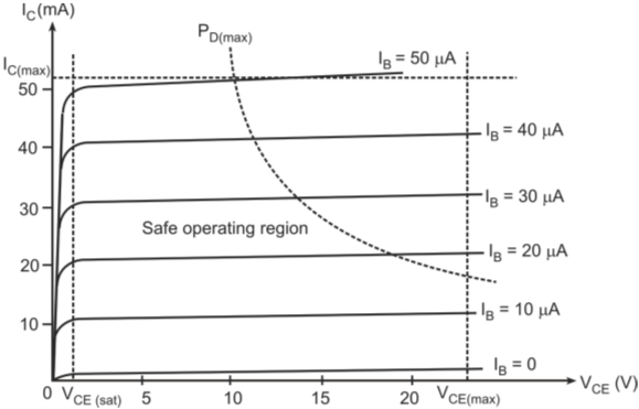
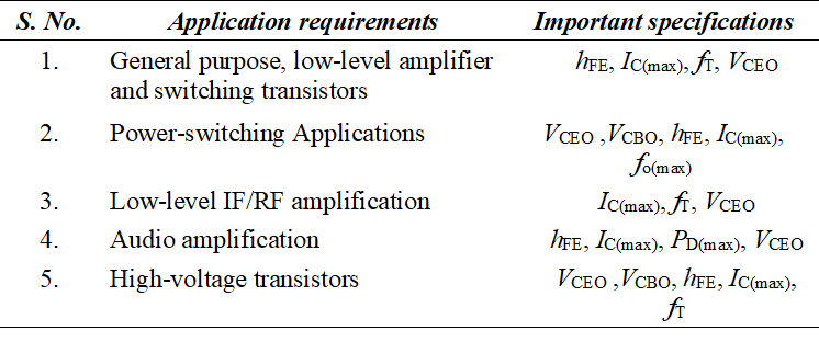
    Some of the important transistor specifications are: DC current gain (β or hFE), AC current gain (βac or hfe), gain-bandwidth product (fT), transistor breakdown voltages and maximum power dissipation (PD(max)).

  • Why is DC Current Gain (β) parameter important for switching transistors?

    β is an important parameter for switching transistors as it tells the minimum base current required to drive the transistor in the saturation region for a certain collector current. For a given collector current, a transistor with smaller hFE needs a harder base drive.

  • Define the term ‘Gain-Bandwidth Product (fT)’ for a transistor?

    ‘Gain-bandwidth product’ is the frequency for which gain on the high-frequency side falls to unity or 0 dB. Therefore, it tells us about the high frequency response of the transistor. It is an important parameter that needs to be considered when the transistor is to be used for IF/RF applications.

  • What are the different breakdown phenomena that can take place in a transistor?

    There are two types of breakdown phenomena possible in a transistor. These are
    • Avalanche breakdown
    • Reach-through phenomenon or the punch-through effect

  • What are the breakdown voltages associated with avalanche multiplication?

    The breakdown voltages associated with the avalanche multiplication are VCEO and VCBO. VCEO is the maximum voltage that can be applied across the collector–emitter junction with the base open in the CE configuration. It is the worst case of collector–emitter breakdown voltage and is a very important specification particularly in switching transistors used in switched-mode power supplies. This parameter is often specified in following different ways.
    • VCER – It is the collector–emitter breakdown voltage with a specified resistance typically of the value of 100–200 Ω connected between the base and emitter
    • VCES – It is the collector–emitter breakdown voltage with base shorted to the emitter
    VCBO is the reverse output breakdown voltage when the transistor is connected in the CB configuration with the emitter terminal open. VCEO is the lowest of all the voltage ratings. and if the design is such that the VCEO rating is not exceeded, the possibility of collector–emitter junction breakdown gets eliminated.

  • Explain the transistor breakdown due to reach-through effect?

    Due to reach-through effect, the width of the collector–base junction depletion region increases with increase in the reverse voltage. As the base region is very thin, even at moderate values of reverse voltages, the depletion region spreads completely across the base and reaches the emitter junction. This results in large flow of emitter current leading to transistor breakdown. The collector–base breakdown voltage due to the punch-through effect is independent of the transistor configuration.

  • What is safe operating area of the transistor?

    Refer figure below. The maximum collector current (IC(max)), collector–emitter voltage (VCE(max)) and the power ratings (PD(max)) limit the active region of operation of a transistor. VCE(sat) specifies the minimum collector–emitter voltage required to drive the transistor in the active region. The area enclosed by dotted lines represents the safe operating area of the transistor.

    Safe operating region of a transistor

  • List different application areas of a transistor and the specifications relevant to each of the applications?

    Table below lists the typical transistor applications and important specifications

Got a voltage spike of curiosity?

Send your doubts now!