Common Base Configuration

  • What is a common base (CB) configuration?

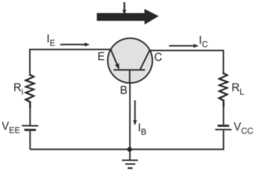
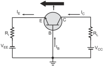
    In this configuration, the base terminal is common to both the input and the output sections. Figures below show the basic circuit of the transistor in the CB configuration for the NPN and the PNP transistors. The directions of currents shown are used for conventional current flow. Please note that the current flowing into the transistor is taken as positive and the current leaving the transistor is taken as negative.

    Common-base configuration for NPN transistor

    Common-base configuration for PNP transistor

  • Draw the input characteristics of a transistor in CB configuration?

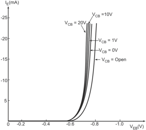
    The input characteristics of CB configuration relate the emitter current ( IE ) to the emitter–base voltage (VEB) for various levels of the collector–base voltage (VCB). The current IE is considered negative as the current flows out of the emitter terminal. Figure below shows the input characteristics of a common-base NPN Silicon transistor. Please remember that the input characteristics of PNP transistors are same with the reversal of polarity of the voltages and currents.

    Input characteristics of CB NPN Si transistor

    From the figure we can infer the following

    • There is a cut-in or threshold voltage below which the value of emitter current is very small.
    • Typical values of cut-in voltage for Silicon and Germanium transistors are approximately 0.5 and 0.1 V respectively.
    • The input characteristic curve for open condition is the same as that for a forward-biased PN junction diode.
    • For a fixed value of collector–base voltage (VCB), the emitter–base voltage (VEB) increases with increase in the emitter current (IE).
    • Since a small change in the emitter–base voltage causes a very large change in the emitter current, the input resistance (ri) of the common-base configuration is very small (of the order of hundred ohms in the linear portion of the input characteristics)
    • For fixed value of emitter–base voltage (VEB), the emitter current (IE) increases with increase in the collector–base voltage (VCB). This is because of the early effect phenomenon in transistors.

  • What is Early effect phenomenon in transistors?

    Early effect is also known as base width modulation phenomenon. It refers to the change in the width of the base region with the change in the collector–base voltage. The emitter–base junction is forward-biased and hence the width of the depletion region is negligible. For the reverse-biased collector–base junction, the width of the depletion region is substantial. The width of the depletion region increases with increase in the reverse voltage at the collector–base junction. As the base region is lightly doped, the penetration of the depletion region is much larger in the base region than in the collector region. Therefore, the effective width of the base region decreases. This phenomenon of change in the effective width of the base region with change in the collector–base voltage is referred to as the early effect.
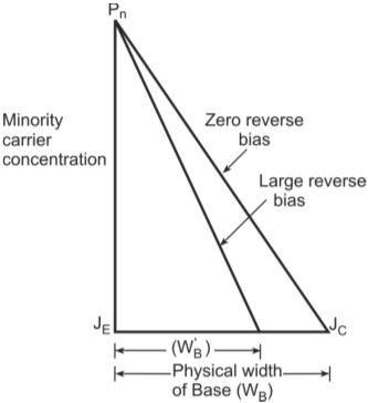
    As a result of the early effect, the rate of recombination of the electrons and holes decreases as the reverse potential is increased. This results in increase in the value of α. Also, the concentration of the minority carriers becomes zero at effective base width (W'B) instead of WB as shown in figure below. Therefore, the concentration gradient of minority carriers (Pn) is increased within the base region. As the emitter current is proportional to the gradient of minority carriers at the emitter junction (JE), the value of emitter current also increases.

    Early effect phenomenon

  • Draw the output characteristics of a transistor in CB configuration.

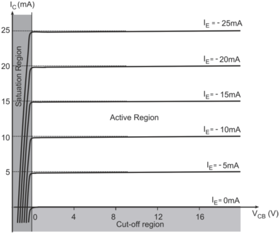
    The output characteristics of common-base configuration are shown in figure below. They relate the collector current (IC) to the collector–base voltage (VCB) for various levels of the emitter current (IE). As we can see from the figure, for a fixed value of emitter current, the collector current almost remains constant with changes in the value of the collector–base voltage. However, near the origin the collector current drops rapidly with the decrease in the value of the collector-base voltage.

    Output characteristics of the common-base transistor

  • How can the output characteristics of a transistor be divided into different operating regions?

    The output characteristics of a transistor can be divided into three regions, namely the active region, the cut-off region and the saturation region.

  • Explain the active region of a common-base transistor?

    For a common-base configuration, in the active region, the collector–base junction is reverse-biased while the emitter–base junction is forward-biased. The unshaded portion of Figure below corresponds to the active region.
    Output characteristics of the common-base transistor

    As we can see from the figure, in the active region, the output characteristics curves are straight parallel lines. It is so because the collector current (IC) is almost independent of the collector–base voltage (VCB) and depends only on the value of the emitter current (IE). The collector current actually increases slowly with the collector–base voltage (around 0.5%) due to the early effect phenomenon. But for most applications this increase can be ignored and the collector current can be considered to be constant for a fixed value of emitter current. The output resistance (ro) offered by the CB configuration is very high as a very large change in the collector–base voltage produces a very small change in the collector current. The lowest curve in the output characteristics corresponds to the situation when the emitter–base junction is open-circuited. Therefore, the emitter current is zero and the collector current that flows in this condition is the reverse saturation current (ICO) (ICO ~ few microamperes for Germanium transistors and several nanoamperes for Silicon transistors).

  • Explain the cut-off region of a common-base transistor?

    For a common-base transistor, in the cut-off region, both the collector–base and the emitter– base junctions are reverse-biased. Refer to figure below.

    Output characteristics of the common-base transistor

    The region below the IE = 0 curve corresponds to the cut-off region. Here, the transistor acts as an open circuit and does not conduct any current. Only a small amount of collector current flows at IE = 0 and is equal to the reverse saturation current (ICO). ICO is also referred to as ICBO, the collector current with base open-circuited. ICBO can be ignored in most transistor applications except for power transistors and transistors operating at high temperatures.

  • What is the relation between the collector reverse saturation current and temperature?

    Collector reverse saturation current increases rapidly with increase in temperature. For a general-purpose Silicon transistor 2N2222, the values of ICO at a collector–base voltage of 50 V for ambient temperatures 25°C and 150°C are 10 nA and 10 μA, respectively. We can see that there is a change of the order of 1000 times for 125°C change in temperature.

  • Explain the saturation region of a common-base transistor?

    For a common-base transistor, in the saturation region, both the collector–base and the emitter–base junctions are forward-biased. The region to the left of VCB = 0 line (refer to figure below) corresponds to the saturation region. In the saturation region, the collector–base voltage (VCB) is slightly negative because the collector–base junction is also forward-biased. There is an exponential increase in the collector current with a small increase in the collector–base voltage.

  • What is the current gain of a common-base transistor?

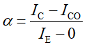
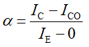
    For a common-base transistor, alpha (α) is referred to as the large-signal current gain. It is the fraction of emitter current that contributes to the collector current. The current equation in a transistor is given by

    The above equation can be rewritten as

    From the above equation, alpha ( α) can be defined as the ratio of the increment in the value of collector current from its value in the cut-off region to the increment in the value of emitter current from its value in the cut-off region. As the value of ICO is very small, it can be ignored in the large-signal analysis. Therefore,

  • What are the typical values of current gain alpha ( α)?

    In the active region, the value of α is nearly equal to 1 (exact value being between 0.90 and 0.998). Therefore, the current gain of the transistor in the CB mode is less than unity.

  • On what parameters does the value of alpha ( α) depend?

    The value of α varies with emitter current (IE), collector voltage (VCB) and operating temperature.

  • A CB transistor acts as a voltage or a current amplifier?

    The voltage gain of the CB configuration is in the range of 50–300, while the current gain is less than 1. Therefore, a CB transistor acts as a voltage amplifier and not as a current amplifier.

  • What do you mean by term ac alpha (αac)?

    αac is the common base, short circuit amplification factor. When a time-varying input is applied to a CB configuration, the point of operation moves on the output characteristics curve. In that case an ac alpha (αac) is defined as the ratio of the change in the collector current to the change in the emitter current for a fixed value of collector–base voltage.

Got a voltage spike of curiosity?

Send your doubts now!