Common Emitter Configuration

  • Which is the most commonly used configuration?

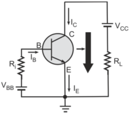
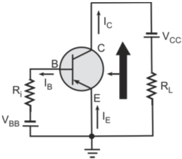
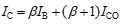
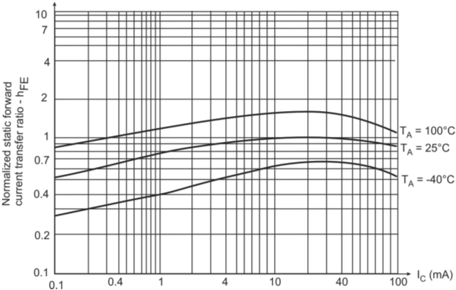
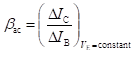
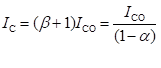
    The common-emitter (CE) configuration is the most commonly used transistor configuration.

  • What is common-emitter configuration?

    Common-emitter configuration has emitter terminal common to both the input and the output sections. The input signal is applied to the base–emitter section and the output is taken from the collector–emitter section. Figures below show the CE configuration for the NPN and the PNP transistors, respectively. Salient features of CE transistor configuration are high values of voltage and current gains, medium values of input and output impedances.

    Common-emitter configuration for NPN transistor

    Common-emitter configuration for PNP transistor

  • Draw the input characteristics of a transistor in CE configuration?

    The input characteristics of a CE transistor (refer to figure below) relate the base current (IB) to the base–emitter voltage (VBE) for different values of the collector–emitter voltage (VCE). We can infer the following from the input characteristics of a CE transistor.

    • Magnitude of base current (IB) is in range of several tens of microamperes
    • An increase in the value of collector–emitter voltage (VCE) results in a decrease in the value of the base current (IB), for fixed values of base–emitter voltage (VBE). This is because of the early effect which results in reduction of the base width with increase in the collector–emitter voltage (VCE).

    Input characteristics of a CE transistor

  • Draw the output characteristics of a transistor in CE configuration?

    Output characteristics of the CE configuration (refer to figure below) relate the collector current (IC) to the collector–emitter voltage (VCE) for different values of base current (IB).

    Output characteristics of a CE transistor

    As we can see from the figure, the output curves for CE configuration are not as horizontal as that for CB configuration. This indicates that the collector–emitter voltage has an influence on the value of collector current.

  • Define Beta (β) of a transistor?

    For any transistor, the emitter, collector and base currents are related to each other as given below

    As the value of ICO is very small,

    Therefore, β is defined as the DC forward current transfer ratio or the DC current gain of the transistor. It is also denoted as hFE. Typical value of β is in the range of 50–100.

  • Give reasons why as to a very small change in the value of α is reflected as a very large change in the value of β?

    α and β are related to each other by the equation

    Therefore, a very small change in α is reflected as a very large change in β.

  • On what parameters does the value of β depend?

    The value of β varies considerably with changes in both the operating temperature and collector current (Refer to figure below). It also varies from one transistor to another transistor of the same type number.

    Variation of β with change in temperature and collector current

  • Define the characteristics of a CE transistor configuration in the active region?

    As in the case of CB transistor configuration, for CE transistor configuration also, the collector–base junction is reverse-biased while the emitter–base junction is forward-biased. The active region characteristics (refer to figure below) corresponds to the portion of the graph to the right of the line at VCE(sat) and above the curve for IB = 0.

    Output characteristics of a CE transistor

  • What are the typical applications of CE mode transistors in the active region?

    Transistors in the CE configuration have high value of current gain, voltage gain and power gain. Hence, they are used as voltage, current and power amplifiers.

  • What do you understand by the term ac beta?

    The term ac beta is defined for AC applications. For AC applications ac beta ((βac) is defined as

    βac is referred to as the CE forward-current amplification factor and is also denoted by hFE.

  • Define the characteristics of a CE transistor in saturation region?

    A CE transistor is in the saturation region when both the collector–base and the emitter–base junctions are forward-biased. Therefore, collector–base voltage (VCB) and emitter–base voltage (VEB) are equal to the cut-in voltages of the base–collector and the base–emitter junctions, respectively. The value of VCE (VCB-VBE) is few tenths of volts in the saturation region. Saturation region corresponds to the region left of VCE = VCE(sat) line in the output characteristics. In the saturation region, the value of the collector current is independent of the base current and depends on the value of resistor connected between the collector terminal and the supply terminal.

  • For the CE circuit shown in figure below, what is the minimum base current required to saturate the transistor? What is the value of the collector current in the saturation region?

    Transistor in CE configuration

    For the given figure, value of collector current in the saturation region is given by IC = VCC/RL. The minimum base current required to saturate the transistor is given by IC/hFE.

  • Which parameters are of importance in the CE configuration saturation mode transistor?

    CE saturation resistance (RCE(sat)) is defined as the ratio of the collector–emitter voltage at saturation to the collector current (VCE(sat)/IC). The curves to the left of the VCE = VCE(sat) line can be approximated as straight lines whose slope can be determined using the value of RCE(sat). Therefore, the CE saturation resistance parameter is of utmost importance in the saturation mode of a CE configuration transistor.

  • Define the characteristics of a CE transistor in the cut-off region?

    In the cut-off region, both the collector–base and the emitter–base junctions are reverse-biased. The base current is equal to zero (IB = 0) in this region. The collector current flowing through the transistor is then given by

    This current is denoted by the symbol ICEO.

  • A Silicon transistor is in the cut-off region when IB = 0 both for short circuit (VBE = 0) and reverse-biased base–emitter junction. Given reasons why?

    For Silicon transistors, the value of α near cut-off region is nearly zero and therefore, the value of collector current is equal to ICO. Hence, the Silicon transistor is in the cut-off region when IB = 0 both for short circuit (VBE = 0) and reverse-biased base–emitter junction.

  • Germanium transistor is in cut-off region when IB = 0 for reverse-biased base–emitter junction with VBE greater than 0.1 V. Give reasons why?

    For Germanium transistors, the value of α near cut-off region can be as large as 0.9. Therefore, the value of the collector current flowing through the transistor can be as large as 10 times the value of leakage current ICO. This leads to Germanium transistor not being in the cut-off region for IB = 0. A reverse bias needs to be applied to the base–emitter junction to bring the value of collector current (IC) less than or equal to reverse saturation current (ICO) and hence driving the transistor to cut-off. Reverse-bias voltage of 0.1 V is sufficient to reduce the collector current to this value and bring the transistor to cut-off. Therefore, a Germanium transistor is in cut-off region when IB = 0 for reverse-biased base–emitter junction with VBE greater than 0.1 V.

Got a voltage spike of curiosity?

Send your doubts now!