Transistor Construction Techniques

  • Name some of the important transistor construction techniques?

    Some of the important transistor construction techniques are point contact, grown-junction, alloy-junction, diffusion, epitaxial and annular techniques.

  • What are point-contact transistors?

    Point-contact transistors are constructed by placing two wires into the semiconductor wafer. The wires are N-type and the wafer is P-type for an NPN transistor and vice versa for a PNP transistor. Figure below shows an NPN point- contact transistor. Electrical pulses are applied to each of the wire to form a PN junction between the wire and the wafer. The earliest transistors fabricated were point-contact transistors but they are no longer used as they suffer from poor reliability.

    Point-contact NPN transistor

  • What are grown-junction type transistors?

    Refer to figure below.

    Grown-junction type transistors

    Grown-junction type transistors are fabricated from a single crystal drawn from a melt of Silicon or Germanium. The impurity concentration is changed by adding the N-type and the P-type dopants during the crystal drawing operation. The crystal is then sliced into a large number of devices and the contacts are then made as shown in the figure above.

  • What are alloy-junction transistors?

    Alloy-junction transistors have the base as a thin wafer and two dots of impurity elements are placed on opposite sides of this wafer. In the case of an NPN transistor the wafer is a P-type material and the dots are of N-type material (refer to figure below). For a PNP transistor, the wafer is an N-type material and the dots are of P-type material. Temperature of whole structure is raised for a short time to melt the impurity into the base material. The collector region is made larger than the emitter region so that the collector collects maximum number of majority carriers from the emitter region and prevents them from diffusing into the base.

    NPN alloy junction transistor

  • What are diffusion transistors?

    Diffusion technique is the most frequently used technique for transistor fabrication. Here, the semiconductor wafer is subjected to gaseous diffusions of both N-type and P-type impurities to form the emitter–base and the collector–base junctions. Two types of transistors are fabricated using the diffusion technique namely, • Planar transistors • Mesa transistors Planar transistor: Planar diffusion NPN Silicon transistor is shown in figure below. The base–collector region is photo-etched on the block of N-type Silicon and a P-type base region is formed by a gaseous diffusion-masking process. The emitter is then diffused onto the base and the whole structure is covered by a layer of Silicon oxide.

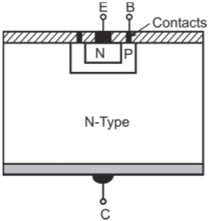
    Planar diffusion transistor

    Mesa transistor: It is basically a planar transistor that has been etched at the base–collector junction leaving a mesa or a flat-topped peak as shown in the figure below. These transistors are rugged devices with high power-dissipation capability and can operate at higher frequencies. However, they have higher value of saturation voltage because of highly resistive collector region and are unsuitable for switching applications

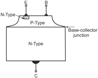
    Mesa diffusion transistors

  • What are epitaxial transistors?

    Both planar and mesa transistors can be constructed using this technique. It consists of growing a very thin, high purity, single-crystal layer of Silicon or Germanium on a heavily doped substrate of the same material. This augmented crystal forms the collector on which the base and the emitter regions are diffused.

  • What are annular transistors?

    In annular transistors, a heavily doped ring (of P-type material for PNP transistors and of the N-type for NPN transistors) is introduced around the base region. The ring interrupts the induced channel and isolates the collector–base junction from the surface of the device. It is therefore a high-voltage device with low collector–base leakage. Figure below shows a PNP annular transistor.

    PNP annular transistor

Got a voltage spike of curiosity?

Send your doubts now!