JFET Common Drain Biasing Configurations

  • Write the advantages of common-drain configuration?

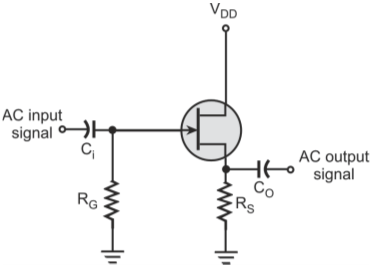
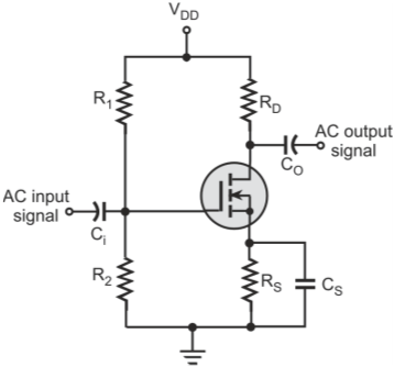
    Similar to the common-collector configuration, the common-drain configuration also offers high input impedance, low output impedance, nearly unity voltage gain and no input–output phase reversal.

  • Draw the circuit diagram of the common-drain configuration for an n-channel JFET?

    Common-drain configuration is also referred to as the source follower configuration. The basic circuit for the common-drain configuration is shown in figure below. The voltage across resistor RS provides the gate-source biasing voltage. The output is taken from the source terminal.

    Common-drain configuration for n-channel JFET

  • What is common-gate configuration?

    In common-gate configuration, the input is applied between the source and the gate terminals and the output is taken between the drain and the gate terminals. The gate terminal is common between the input and the output sections.

  • What are the features of common-gate configuration?

    Common-gate configuration offers low input impedance, high output impedance, high voltage gain and the output voltage is in phase with the input voltage.

  • Draw the circuit for common-gate configuration for an n-channel JFET?

    Figure below shows the circuit diagram for common-gate configuration for an n-channel JFET.

    Common-gate configuration

  • Write the voltage and current equations for common-gate configuration for an n-channel JFET?

    The values of the gate-source and drain-source voltages are given by the following equations respectively.

  • Compare the biasing configurations used for JFETs and DE-MOSFETs?

    DE-MOSFETs and JFETs have similarities in their characteristics. Therefore, their biasing configurations are also the same. The only difference being that DE-MOSFETs also operate in enhancement mode, that is, with positive values of gate-source voltage (VGS) in addition to the depletion mode.

  • What are the popular biasing configurations for E-MOSFETs?

    Two most popular biasing configurations for E-MOSFETs are the feedback biasing configuration and the voltage-divider configuration.

  • Explain the feedback biasing configuration for E-MOSFETs?

    Figure below shows the circuit for the feedback biasing configuration. The feedback connection to the gate terminal is taken from the drain terminal through resistor RG. The resistor RG feeds bias voltage to the gate terminal to turn the MOSFET ON.

    Feedback biasing configuration for E-MOSFET

  • Perform the DC analysis for the feedback biasing configuration for E-MOSFETs?

    Figure below shows the DC equivalent circuit for the feedback biasing configuration for E-MOSFET. Since the gate current (IG) is approximately equal to zero, therefore the voltage drop across resistor RG is also approximately equal to zero.

    DC equivalent of the circuit

    Applying Kirchhoff’s voltage law to the input section we get

    Therefore, gate-source voltage (VGS) is given by

    Applying Kirchhoff’s voltage law to the output section and solving for the drain-source voltage (VDS) we get

    From the above equations,

  • How to determine the operating point for feedback biasing configuration for E-MOSFETs?

    The operating point can be obtained by solving the equations in question 28. It can also be established using graphical method as shown in Figure below. The figure shows that the straight line given by equation is superimposed on the transfer characteristics of the MOSFET. The point of intersection between the straight line and the transfer curve gives the value of the quiescent gate-source voltage and quiescent drain current. The operating point can also be obtained by superimposing the DC load line defined by equation on the output characteristic curves for the MOSFET.

    Graphical method for determining the operating point for feedback biasing configuration for n-channel E-MOSFET

  • Draw the voltage-divider biasing configuration for E-MOSFETs?

    Figure below shows the circuit for voltage-divider biasing configuration for E-MOSFETs. The arrangement is the same as that for BJTs and JFETs.

    Voltage-divider biasing configuration for E-MOSFET

  • What is the major advantage of FETs over BJTs?

    FETs offer very high input impedance as compared to BJTs. Therefore, they do not load the input source.

  • What are the major applications of FETs?

    FETs are widely used as input amplifiers in oscilloscopes, electronic voltmeters and other test and measurement instruments, as low-noise amplifiers in front end of TV and radio receivers. FETs in the common-drain configuration are used as buffer amplifiers. E-MOSFETs are very commonly used in the fabrication of integrated circuits. FETs are used in switching applications and as voltage variable resistors (VVRs) in operational amplifiers.

  • Explain the use of FET devices as amplifiers?

    FET devices are commonly used as low-noise amplifiers and as buffer amplifiers. FETs are low-noise devices and hence they are used in the front-end of receivers and other electronic equipment and systems. JFETs in common-drain configuration offer high input impedance and low output impedance and hence they are used as buffer amplifiers to isolate the preceding stage from the following stage.

  • How can we use JFETs as analog switches?

    Figure below shows an analog switch using an n-channel JFET. When no gate voltage (VGG) is applied, the FET operates in the saturation region and acts as a closed switch. When a negative gate voltage (VGG) is applied, the FET operates in the cut-off region. Therefore, it offers a very high resistance and acts as an open switch.

    JFET as an analog switch

  • How can we use JFETs as multiplexers?

    Figure below shows an n-channel JFET-based multiplexer. The input signals are applied to the drain terminals of the JFETs while the corresponding control inputs are applied to the gate terminal of the JFETs. When the control input corresponding to one of the input channels is made zero, that input is transmitted to the output. The control inputs for the other channels are made more negative than the VGS(off) voltage. Hence all the other input signals are blocked.

    JFET as a multiplexer

  • How can we use JFETs as current limiters?

    Figure below shows an n-JFET based current limiter. During the normal operation of the circuit, the JFET acts in the ohmic region. When the load current increases substantially due to short circuit or any other reason, the JFET operates in the saturation region. Hence it acts as a constant current source and prevents excessive current through the load.

    n-JFET based current limiter

Got a voltage spike of curiosity?

Send your doubts now!