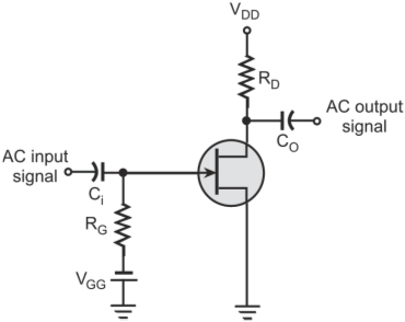
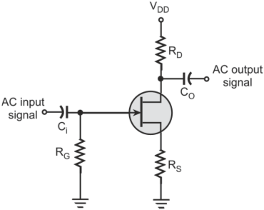
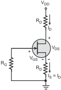
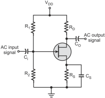
Figure below shows the DC equivalent of a fixed-bias circuit.
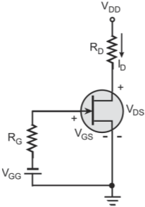
DC equivalent of fixed-bias circuit
In a JFET, gate current (IG) is approximately equal to zero (IG ≅ 0 ). Therefore, the voltage drop across resistor RG is approximately zero.
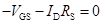
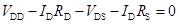
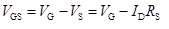
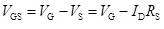
Applying Kirchhoff’s voltage law to the input section we get
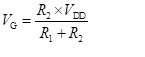
Therefore, the value of gate-source voltage is given by
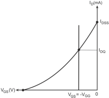
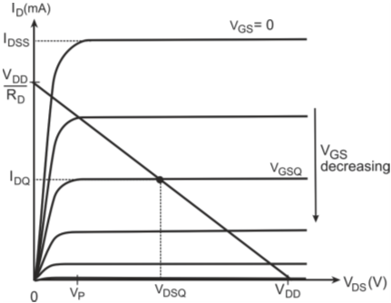
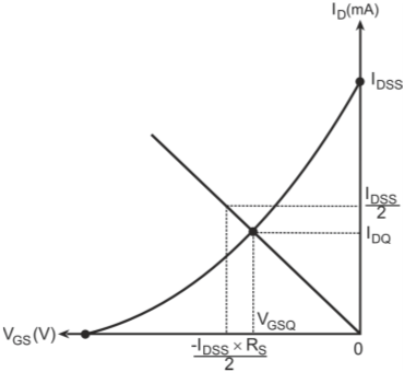
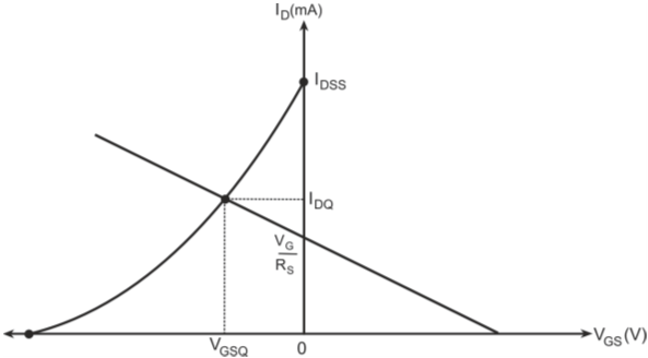
The gate-source voltage (VGS) is negative and equal in magnitude to the applied gate voltage (VGG). As the voltage VGG is fixed, VGS is also fixed. Therefore, the configuration is named as fixed-bias configuration. This value of gate-source voltage is denoted as VGSQ.
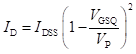
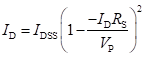
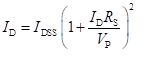
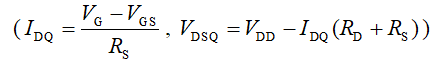
Quiescent drain current (IDQ) is given by
Since the value of gate-source voltage (VGS) in this configuration is fixed, therefore the level of drain current (ID) is also fixed.
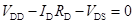
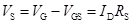
Applying Kirchhoff’s voltage law to the output section we get
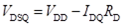
Therefore, the value of quiescent drain-source voltage is given by