VMOS

  • How can the power handling capacity of a MOSFET be increased?

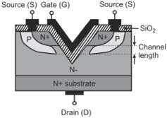
    Power-handling capacity of a MOSFET can be increased by modifying the construction of the MOSFET as shown below. MOSFET with this construction is referred to as vertical metal-oxide-silicon (VMOS) FET or as power MOSFET. Therefore, VMOS has a vertical structure with the channel formed in the vertical direction rather than the horizontal direction.

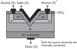
    Structure of a VMOS device

  • Explain the operation of a VMOS device?

    The operation of a VMOS device is similar to that of an E-MOSFET. No channel exists between drain and source terminals and no drain current flows until the gate-source voltage is made positive.

    For positive values of gate-source voltage, an n-channel is formed close to the gate as in case of an E-MOSFET. This is shown in the figure below. The channel is formed in the vertical direction which lets the current carriers to flow between the source and the drain terminals.

    Operation of a VMOS device

  • Draw the characteristic curves for VMOS?

    Drain and transfer characteristics of VMOS are the same as shown in case of planar E-MOSFETs.

  • Why do VMOS devices have lower power-dissipation levels as compared to MOSFETs?

    VMOS devices have smaller channel lengths and larger contact area between the channel and the n+ doped regions as compared to MOSFETs. This results in reduced resistance levels and therefore in reduced power-dissipation levels.

  • Why do VMOS devices have higher current ratings than MOSFETs?

    VMOS devices have higher current ratings than MOSFETs because they have two conductive paths from the drain to the source.

  • Why do VMOS devices have faster switching times as compared to MOSFETs?

    VMOS devices have faster switching times as compared to that of planar MOSFETs as they have reduced charge storage levels.

Got a voltage spike of curiosity?

Send your doubts now!