Regulators

  • What is the role of regulator circuit in a power supply?

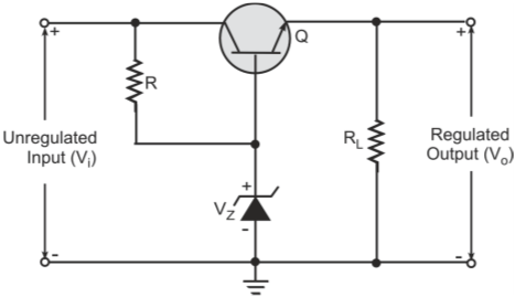
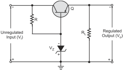
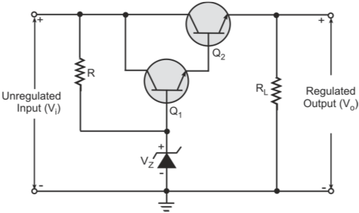
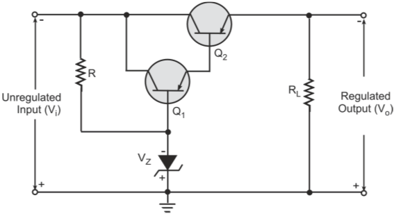
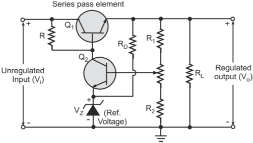
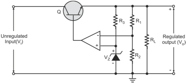
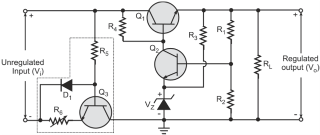
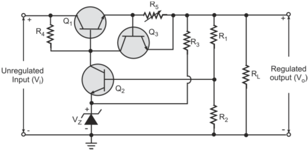
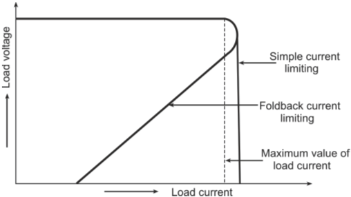
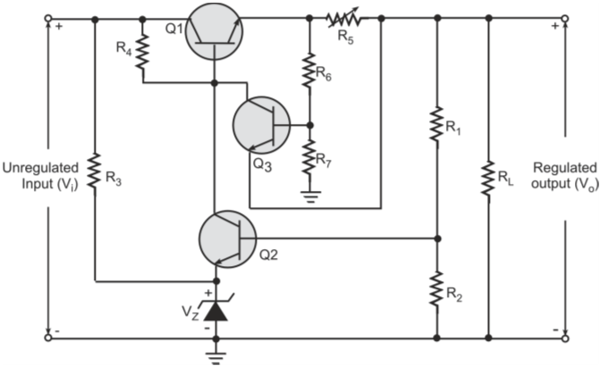
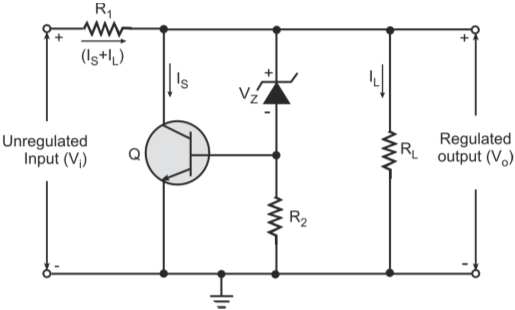
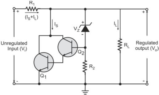
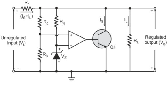
    Regulator circuit in the power supply ensures that the load voltage (in the case of voltage regulated power supplies) or the load current (in the case of current regulated power supplies) is constant irrespective of variations in line voltage or load resistance.

  • In which region does the active device used in the regulator of a linearly regulated power supply operate?

    The active device used in the regulator of a linearly regulated power supply (usually a bipolar transistor) is operated anywhere between cut-off and saturation.

  • List the three types of linear voltage regulator circuits?

    Three basic types of linear voltage regulator configurations include the following.

    • Emitter-follower regulator
    • Series-pass regulator
    • Shunt regulator

  • What are three terminal regulators?

    Emitter-follower and series-pass regulators are available in IC packages in both fixed output voltage as well as variable output voltage varieties. These are popularly known as three terminal regulators.

  • Draw the circuit diagram of a basic positive output emitter-follower regulator? Explain its working?

    Figure below shows the basic positive output emitter-follower regulator. The circuit works as follows.

    • The emitter voltage, which is also the output voltage, remains constant as long as the base voltage is held constant.
    • A Zener diode is connected at the base to hold the base voltage constant.
    • Assuming the base-emitter voltage of the transistor to be 0.6 V, the regulated output voltage in this case is (VZ – 0.6) V.
    • When the output voltage tends to increase, the base-emitter voltage of the series transistor decreases thus decreasing its conduction.
    • This increases collector–emitter drop across the transistor to maintain a constant output voltage.
    • When the output voltage tends to decrease, the base-emitter voltage increases thus increasing the conduction of the transistor. • This decreases the collector–emitter drop across the transistor again maintaining a constant output voltage.
    • Owing to high inherent current gain of the series pass transistor, a low-power Zener diode can be used to regulate high value of load current.
    • The base current need only be [1/(1+hfe)] times the load current.

    Emitter-follower regulator for positive output voltages

  • Draw the circuit diagram of a basic negative output emitter-follower regulator?

    Figure below shows the emitter-follower regulator circuit for negative output voltages.

    Emitter-follower regulator for negative output voltage

    The regulated output voltage in this case is – (VZ – 0.6) V.

  • In Q5, if the load current is beyond the capability of a Zener diode to provide the requisite base current, what needs to be done?

    . If the load current is beyond the capability of a Zener diode to provide the requisite base current a Darlington combination can be used instead of a single transistor series-pass element. Figure below shows the positive output emitter-follower regulator using Darlington transistor. The regulated output voltage is given by (VZ – 1.2) V.

    Emitter-follower regulator using Darlington (positive output)

  • In Q6, if the load current is beyond the capability of a Zener diode to provide the requisite base current, what needs to be done?

    If the load current is beyond the capability of a Zener diode to provide the requisite base current a Darlington combination can be used instead of a single transistor series-pass element. Figure below shows the negative output emitter-follower regulator using Darlington transistor. The regulated output voltage is given by - (VZ – 1.2) V.

    Emitter-follower regulator using Darlington (negative output)

  • . Is the emitter-follower regulator circuit a type of series-pass regulator?

    The emitter-follower regulator circuit is a type of series-pass regulator where the conduction of the series transistor decides the voltage drop across it and hence the output voltage. The Zener diode provides the reference voltage that controls the conduction of the transistor depending upon the output voltage.

  • . Draw the circuit of an improved series-pass-type linear regulator that is capable of providing much better regulation specifications?

    Figure below shows an improved series-pass regulator. These regulators have error amplifiers. As compared to the emitter-follower type series-pass regulator, these regulators provide better regulation due to the gain provided by the error amplifier. Therefore, a given change in output voltage causes a relatively much larger change in the base current of the series-pass element.

    Series-pass linear regulator

    The circuit functions as follows.

    • The series-pass element is a bipolar transistor which works like a variable resistance.
    • Conduction of the transistor depending upon the base current.
    • A small fraction of the output voltage is compared with a known reference DC voltage.
    • This difference is amplified in a high-gain DC amplifier.
    • The amplified error signal is fed back to the base of the series-pass transistor.
    • This alters its conduction so as to maintain essentially a constant output voltage.
    • The regulated output voltage in this case is given by VREF × (R1 + R2)/R2.
    • When there is a decrease in input voltage or increase in load current, the output voltage tends to decrease.
    • The error voltage produced as a result of this causes the base current to increase.
    • The increased base current increases transistor conduction
    • This reduces the collector–emitter voltage drop of the transistor, which compensates for the reduction in the output voltage.
    • When there is an increase in input voltage or decrease in load current, the output voltage tends to increase.
    • The error voltage produced tends to decrease transistor conduction thus increasing its collector emitter voltage drop again maintaining a constant output voltage.
    • The regulation provided by this circuit depends upon the stability of the reference voltage and the gain of the DC amplifier.

  • Draw the circuit of a series pass regulator with BJT as the error amplifier?

    Figure below shows a series pass regulator circuit using a bipolar transistor as the error amplifier.

    Series-pass linear regulator using bipolar transistor as error amplifier

  • . Draw the circuit of a series pass regulator with operational amplifier as the error amplifier?

    Figure below shows a series pass regulator circuit using an operational amplifier as the error amplifier.

    Series-pass linear regulator using opamp as error amplifier

  • What are typical protection features built into a power supply?

    Typical protection features built into a power supply are current limiting protection, crowbaring and thermal shutdown.

  • Why is current limiting protection required in linear power supplies?

    The power dissipated in the series-pass transistor of a linear regulator is the product of its collector–emitter voltage and the load current. The series-pass transistor is so chosen that it can safely dissipate the power under normal load conditions. If there is an overload condition the transistor is likely to get damaged if such a condition is allowed persist for long. If there were a short circuit on the output, the whole unregulated input would appear across the series-pass element. This would increase the power dissipation to prohibitively large magnitude eventually destroying the transistor. Even a series-connected fuse does not help in such a case, as the thermal time constant of the transistor is much smaller than that of the fuse. Therefore, we need to build overload protection or current limiting protection in the linearly regulated power supply design.

  • Draw the circuit of a series-pass regulator with current limiting protection?

    Figure below shows a circuit of a series-pass regulator with current limiting protection.

    Under normal operating conditions, transistor Q3 is in saturation. Thus, it offers very little resistance to the load current path. In the event of an overload or a short circuit, the circuit functions as follows.

    • Under overload conditions, diode D1 conducts thus reducing the base drive to transistor Q3.
    • Transistor Q3 comes out of saturation and offers an increased resistance to the flow of load current.
    • In the event of a short circuit, the whole of input voltage would appear across Q3.
    • Transistor Q3 is so chosen that it can safely dissipate power given by the product of worst-case unregulated input voltage and the limiting value of current.
    • Diode D1 and transistor Q3 are preferably mounted on the same heat sink so that base-emitter junction of Q3 and diode’s P-N junction are equally affected by temperature rise and the short circuit limiting current is as per the preset value.

    Series-pass linear regulator with overload protection

  • . Draw the circuit of another series-pass regulator with current limiting protection?

    Figure below shows a circuit of a series-pass regulator with current limiting and overload protection.

    Series-pass linear regulator with overload protection

    When the load current is less than the limiting value, the circuit regulates the output voltage normally. Transistor (Q3) is in cut-off state. As the load current reaches the limiting value, which is determined by resistor R5, transistor Q3 conducts and the major part of Q1 base current gets routed through Q3 substantially reducing its base drive.

  • What are the disadvantages of the protection circuits discussed in Q15 and Q16?

    Both the circuits discussed in Q15 and Q16 suffer from the disadvantage of large power dissipation in the series-pass transistor in the event of an output short circuit. The power dissipated in the series-pass transistor is approximately equal to the product of the unregulated input voltage and the limiting value of the load current.

  • How can the disadvantage mentioned in Q17 be removed?

    The disadvantage mentioned in Q17 can be removed by using foldback current limiting. It is a form of over-current protection where the load current reduces to a small fraction of the limiting value the moment the load current exceeds the limiting value. This helps in drastically reducing the dissipation in series-pass transistor in the case of short circuit condition. Figure below shows a comparison of voltage versus load current curve in the case of conventional simple current limiting and foldback current limiting.

    Simple current limiting vs foldback current limiting

  • Draw the circuit of a series-pass regulator with foldback current-limiting feature?

    Figure below shows the circuit of a series-pass regulator with foldback current-limiting feature. As we can see from the figure, the base of the current-limiting transistor Q3 is fed from a potential divider arrangement of R6 and R7.

    Series regulator with foldback current limiting

  • Explain the working of the foldback current limiting circuit in Q19?

    In the event of a short circuit, Vo = 0. Therefore, the short-circuit load current (ISL) is the one that produces a voltage equal to VBE (min) required for conduction of current-limiting transistor Q3. That is,

    Where,

    This gives

    When the output is not shorted, potential of Q3 emitter terminal is Vo. Therefore, potential of its base terminal is given by

    Therefore, maximum value of load current (Imax) under these conditions is given by

    Solving the above equation, we get

    The above equation shows that the maximum load current or the limiting value of the load current is larger than the short-circuit current. Typical value of K is such that the maximum load current is about two to three times the short-circuit load current.

  • What is crowbarring?

    Crowbaring is a type of over voltage protection and thermal shutdown protection that disconnects the input to the regulator circuit if temperature of the active device(s) exceeding a certain upper limit.

  • What is a shunt regulator?

    In a shunt regulator, regulation is provided by a change in the current through the shunt transistor to maintain a constant output voltage. Figure below shows a simple shunt regulator circuit.

    Shunt regulator

    The regulated output voltage here is the unregulated input voltage minus drop across a resistance R1. As the output voltage tends to decrease, the base current through the transistor reduces with the result that its collector current (Is) decreases too. This reduces the voltage drop across R1 and the output voltage is restored to its nominal value. Similarly, the tendency of the output voltage to increase is accompanied by an increase in current through the shunt transistor consequently increasing voltage drop across R1, which in turn maintains a constant output voltage.

    Regulated output voltage of this circuit is (VZ + VBE).

  • How can the current capability of the shunt regulator of Q22 be enhanced?

    The current capability of the shunt regulator of Q22 can be enhanced by using a Darlington combination in place of shunt transistor. Figure below shows the circuit.

    Regulated output voltages of this circuit is (VZ + 2VBE).

    Shunt regulator with Darlington arrangement

  • Draw the circuit diagram of an op-amp based shunt regulator?

    Figure below shows the circuit diagram of an op-amp based shunt regulator. Input terminals of the op-amp are fed with reference voltage and the sample of output voltage. The op-amp output drives the base terminal of the shunt transistor. If the input voltages to the op-amp differ, the output of opamp forces the shunt element to conduct more or less current through it thus maintaining a constant output voltage.

    Opamp-based shunt regulator circuit

  • What are the advantages of a shunt regulator over a series regulator?

    Shunt regulators have a simple design and they are inherently protected against overload conditions.

  • What are the disadvantages of a shunt regulator as compared to a series regulator?

    Shunt regulators are less efficient as compared to series regulators. This is so because the current through the series resistor in the case of shunt regulator is the sum of load current and shunt transistor current and it dissipates more power than the series-pass regulator with same unregulated input and regulated output specifications. In a shunt regulator, the shunt transistor also dissipates power in addition to the power dissipated in the series resistor.

Got a voltage spike of curiosity?

Send your doubts now!