High-Frequency Response of FET Amplifiers

  • Draw the high frequency model for a FET?

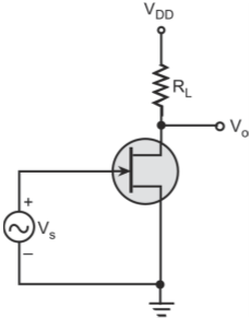
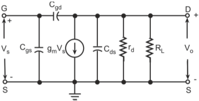
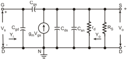
    High-frequency response of an FET amplifier is similar to that of a BJT amplifier. Figure below shows the high-frequency model for an FET (JFET as well as MOSFET). As we can see from the figure, the high-frequency model is similar to the low-frequency model with the addition of junction capacitances.

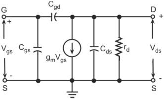
    High-frequency model of a FET

    The capacitance Cgs represents the barrier capacitance between the gate and the source terminals. Cgd is the barrier capacitance between the gate and the drain terminals. Cds is the drain-to-source capacitance of the channel. These capacitors offer high impedance at lower frequencies and can be considered as open circuit. However, at high frequencies, due to these capacitances feedback exists between the input and output circuits and voltage amplification drops rapidly as the frequency increases.

  • Draw the high-frequency equivalent model for the common-source JFET amplifier shown in figure below?

    Common-source JFET amplifier

    Figure below shows the high-frequency equivalent model for the common-source JFET amplifier.

    High-frequency model for the common-source JFET amplifier

  • Determine the output voltage for the common-source JFET amplifier of Q2?

    Output voltage Vo is given by the product of short-circuit current (I) and the impedance seen among the output terminals (Z). Therefore,

    Z is determined by shorting the input terminals, that is, Vs = 0. Hence, there is no current flowing through the current generator gmVs. Therefore, the value of Z is given by the parallel combination of RL, Cds, rd and Cgd and is given by

    Where, GL = 1/RL is the conductance corresponding to load RL If the load is represented by an impedance ZL, then GL will be replaced by YL (YL is the admittance corresponding to impedance ZL). Also Yds = j ω Cds is the admittance corresponding to Cds; gd = 1/rd is the conductance corresponding to rd; Ygd = j ωCgd is the admittance corresponding to Cgd. The current I flowing from the drain to the source terminal with output terminals shorted is given by

    Therefore, the output voltage Vo is given by

  • Determine the voltage gain for the common-source JFET amplifier of Q2?

    The value of voltage gain (Av) is equal to

    At low frequencies, the FET capacitances can be neglected and hence Yds = Ygd = 0. Therefore, the value of gain at low frequencies is given by

    Where

  • Determine the input admittance and the input capacitance for the common-source JFET amplifier of Q2?

    As we can see from the high-frequency model in Q2 that there is a coupling between the gate and the drain terminals through capacitance Cgd. The admittance offered by the capacitance (Ygd) can be replaced by Ygd(1 – AV) between the gate and the source terminals and by Ygd[1 – (1/AV)] between the drain and the source terminals. The input admittance (Yi) is therefore given by

    The input capacitance (Ci) is given by

  • What is the significance of the input capacitance for the common-source JFET amplifier of Q2?

    Input capacitance is important in the case of cascaded amplifiers where the input impedance of a stage acts in shunt across the output impedance of the preceding stage. As the reactance of a capacitance decreases with frequency, the input impedance decreases and hence the gain of the cascaded amplifier also decreases with increase in frequency.

  • . Determine the output admittance for the common-source JFET amplifier of Q2?

    The output impedance is obtained by the impedance looking into the drain and the source terminals, with the input voltage (Vi) set equal to zero. With Vi = 0, the resistance rd and capacitances Cds and Cgd are in parallel. Therefore, the output admittance (Yo) is given by

  • Draw the high-frequency equivalent model for the common-drain JFET amplifier shown in figure below?

    Common-drain amplifier (source-follower amplifier)

    Figure below shows the small-signal high-frequency equivalent circuit of the common-drain amplifier.

  • . What is the value of voltage gain for the common-drain JFET amplifier of Q8?

    Output voltage Vo is given by the product of the short-circuit current and the impedance between the source and the ground terminals. Voltage gain can be obtained in a manner similar to that for the common-source amplifier. The expression for the voltage gain (Av) for a common-drain amplifier is given by

    At low frequencies, the value of reactance offered by the capacitances Cgs, Cds and Csn is infinity. Therefore, at low frequencies, the value of voltage gain (Av) is given by

    The value of Av is slightly less than unity as generally gmRs >> 1.

  • What is the value of input admittance for the common-drain JFET amplifier of Q8?

    Input admittance (Yi) is obtained by using the Miller’s theorem in a manner similar to that done for the common-source FET amplifier. The expression for (Yi) is given by

    One of the major advantages of the common-drain amplifier over the common-source amplifier is that it offers lower input capacitance as compared to the common-source amplifier.

  • What is the value of input admittance for the common-drain JFET amplifier of Q8?

    The output admittance (Yo) can also be determined in a manner similar to that for the common-drain FET amplifier. It is given by

Got a voltage spike of curiosity?

Send your doubts now!