Opamp Comparators

  • What is a comparator?

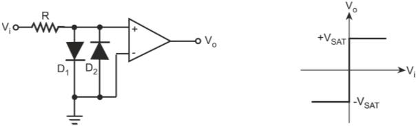
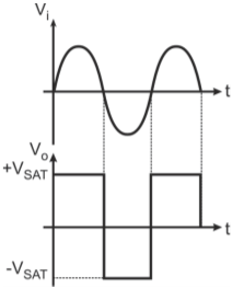
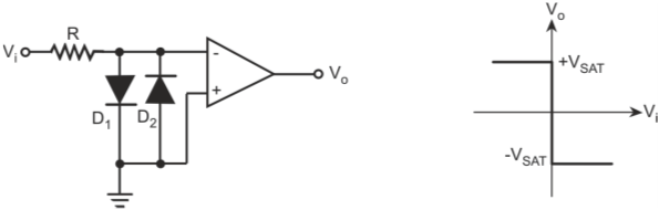
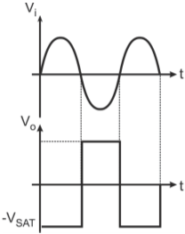
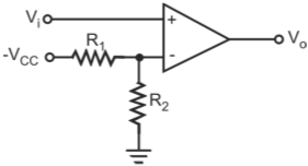
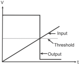
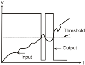
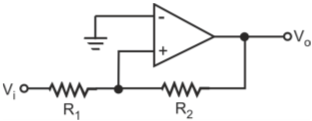
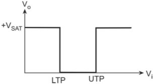
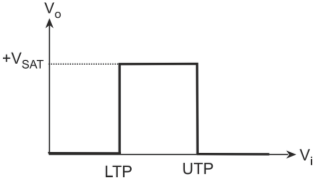
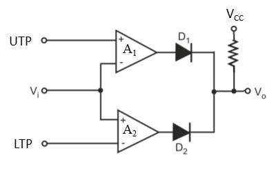
    A comparator circuit is a two-input, one-output building block that produces a high or low output depending upon the relative magnitudes of the two inputs. One of the inputs of the comparator is generally applied a reference voltage and the other input is fed with the input voltage that needs to be compared with the reference voltage.

  • Can we use an opamp as a comparator?

    An opamp can be used as a comparator when used without negative feedback. Because of very large value of open-loop voltage gain, it produces either positively saturated or negatively saturated output voltage depending upon whether the amplitude of the voltage applied at the non-inverting input terminal is more or less positive than the voltage applied at the inverting input terminal. However, it may not be able to produce an output which is compatible with a digital logic family and may have slew rate limitation.

  • What is a zero-crossing detector?

    Zero-crossing detector is a circuit that that changes the output state when the input crosses the zero voltage. The reference voltage in this case is zero. There are two types of zero-crossing detectors namely the non-inverting zero-crossing detector and inverting zero-crossing detector. In a non-inverting zero-crossing detector, an input slightly more positive than zero leads to a positively saturated output voltage whereas in an inverting zero-crossing detector, an input slightly more positive than zero leads to a negatively saturated output voltage.

  • Draw the circuit of a non-inverting zero-crossing detector?

    Figure below shows the basic circuit arrangement of a non-inverting type of zero-crossing detector along with its transfer characteristics.

    Non-inverting zero-crossing detector – circuit and transfer characteristics

    Diodes D1 and D2 connected at the input are to protect the sensitive input circuits inside the opamp from excessively large input voltages. Resistor R is the current-limiting resistor.

  • Draw the input-output waveforms for a non-inverting zero-crossing detector?

    Figure below shows the input-output waveforms for a non-inverting zero-crossing detector

    Non-inverting zero-crossing detector – input and output waveforms

  • Draw the circuit of an inverting zero-crossing detector?

    Figure below shows the basic circuit arrangement of an inverting type of zero-crossing detector along with its transfer characteristics.

    Inverting zero-crossing detector – circuit and transfer characteristics

  • Draw the input-output waveforms for an inverting zero-crossing detector?

    Figure below shows the input-output waveforms for an inverting zero-crossing detector.

    Inverting zero-crossing detector – input and output waveforms

  • What are the applications of zero-crossing detectors?

    Zero-crossing detectors are used in electronic circuits for switching purpose and in phase locked loops. One common application of zero-crossing detector is to convert sine wave signal to a square wave signal.

  • Draw the circuit diagram of a non-inverting comparator for a positive reference voltage?

    Figure below shows the circuit diagram of non-inverting comparator for a positive reference voltage.

    Non-inverting voltage comparator with positive reference

    VREF is given by the equation
    VREF = +VCC × [R2/(R1 + R2)]

  • Draw the circuit diagram of an inverting comparator for a negative reference voltage?

    Figure below shows the circuit diagram of an inverting comparator for a negative reference voltage.

    Non-inverting voltage comparator for negative reference

    VREF is given by the equation
    VREF = -VCC × [R2/(R1 + R2)]

  • What are the advantages of specially designed opamp comparators over general opamps being used as comparators?

    General-purpose opamps when used as comparators suffer from slew rate limitation. Relatively lower slew rate results in prohibitively large transition time from one state to the other. This problem can be overcome by using a high-speed opamp with a higher slew rate specification or by eliminating the compensation capacitor. Even with the slew rate problem solved, general opamps offer other limitations including non-ability to operate from a single supply and interface conveniently with popular logic families. Therefore, we have specially designed opamp comparators to cater to all these requirements.

  • Draw a simplified schematic diagram of an opamp comparator?

    Figure below shows the simplified schematic diagram of opamp comparator. As seen in the figure, the output has an open-collector output stage. For the output stage to work properly, the output terminal needs to be connected to the positive supply voltage through an external resistor called pull-up resistor. However, pull-up resistor slows down the response time of the comparator. Therefore, for faster switching times opamp comparators with active pull-up output stage are used. Limitation of these comparators is that they need dual power supplies.

    Basic circuit schematic arrangement of opamp comparator

  • Draw the output of a comparator for an ideal input signal without noise?

    Figure below shows the output of a comparator for an ideal input signal without noise. Here, the input is considering to be a linearly rising input signal.

    Input-output waveforms of a comparator for an ideal input

  • What happens when the input signal to a comparator is noisy?

    When the input signal to comparator contains noise, transitions at the output around the trip point become highly erratic. Transition around the trip point is not smooth from one state to the other and is a cluster of pulses with randomly varying pulse width specially if the input signal were changing slowly. Figure below shows the input-output transitions for a noisy signal.

    Input-output waveforms of a comparator for a noisy input signal

  • How can the erratic transition problem of a comparator for a noisy input signal be removed?

    The erratic transition problem of a comparator for a noisy input signal can be removed by using a comparator with hysteresis.

  • What is a comparator with hysteresis?

    A comparator with hysteresis uses two different threshold voltages (one for low-to-high transition and another for high-to-low transition) to avoid the erratic transition problem.

  • Draw the circuit schematic of an inverting comparator with hysteresis?

    Figure below shows the circuit schematic of an inverting comparator

    Inverting comparator

    The circuit functions as follows. Let us assume that the output is in positive saturation. Voltage at non-inverting input in this case is VSAT × R1/(R1 + R2). Due to this small positive voltage at the non-inverting input, the output stays in positive saturation. The input signal needs to be more positive than this voltage for the output to go to negative saturation. Therefore, the upper trip point is VSAT × R1/(R1 + R2). Once the output goes to negative saturation, voltage fed back to non-inverting input becomes VSAT × R1/(R1 + R2). Due to this small negative voltage at the non-inverting input, the output stays in negative saturation. The input signal amplitude needs to become more negative than this for the output to go to positive saturation. Therefore, the lower trip point is VSAT × R1/(R1 + R2). In this manner, the circuit offers a hysteresis of 2VSAT × R1/(R1 + R2). Figure below shows the transfer characteristics for an inverting comparator.

    Inverting comparator

  • Draw the circuit schematic of a non-inverting comparator with hysteresis?

    Figure below shows the circuit schematic of a non-inverting comparator with hysteresis. Upper and lower trip points are, respectively, given by +VSAT × R1/R2 and -VSAT × R1/R2. Hysteresis in this case is equal to 2VSAT × R1/R2.

    Non-inverting comparator with hysteresis

  • What is a window comparator?

    In a window comparator, there are two reference voltages called the lower and the upper trip points. Output is in one state when the input is inside the window created by the lower and upper trip points and in the other state when it is outside the window.

  • Draw the circuit diagram of an opamp-based window comparator?

    Figure below shows the basic circuit diagram of a window comparator. When the input voltage is less than the voltage reference corresponding to the lower trip point (LTP), output of opamp A1 is at +VSAT and that of opamp A2 is at -VSAT. Diodes D1 and D2 are respectively forward- and reverse-biased. Consequently, output across RL is at +VSAT.

    Window comparator

    When the input voltage is greater than the reference voltage corresponding to the upper trip point (UTP), the output of opamp A1 is at -VSAT and that of opamp A2 is at +VSAT. Diodes D1 and D2 are respectively reverse- and forward-biased with the result that the output across RL is again at +VSAT. When the input voltage is greater than LTP voltage and lower than UTP voltage, the output of both opamps is at negative saturation with the result that diodes D1 and D2 are reverse-biased and the output across RL is zero. Figure below shows the transfer characteristics of this window comparator.

    window comparator

  • A window comparator has transfer characteristics as shown in figure below. How can these characteristics be obtained?

    .

    The transfer characteristics shown in figure above can be obtained if we interchange the positions of LTPs and UTPs and the comparators used are the ones with an open-collector output. In this case a pull-up resistor will be connected from the output pin of the comparator to the supply terminal. Figure below shows the circuit.

    Window comparator

Got a voltage spike of curiosity?

Send your doubts now!