Semiconductor Diode VI Characteristics

  • What do you mean by the term “Ideal Diode”?

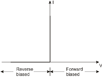
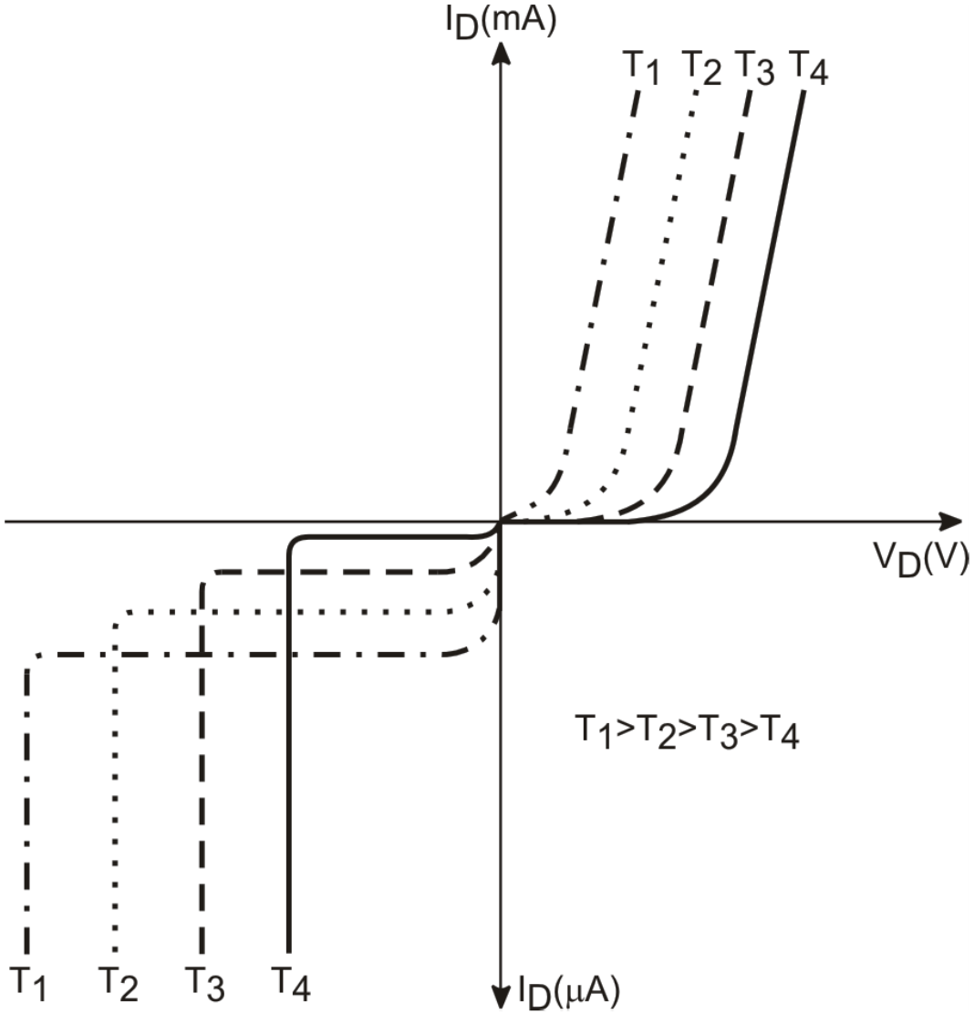
    An ideal diode acts as a short circuit (zero ON-resistance) when forward-biased and as an open circuit (infinite OFF-resistance) when reverse-biased. In other words, it behaves like a switch that conducts current only in one direction, from anode to cathode

  • Draw the V-I characteristics of an ideal diode.

    Figure below shows the V-I characteristics of an ideal diode.

    V-I characteristics of an ideal diode

  • How does a practical diode differ from an ideal diode?

    The differences between ideal and practical diodes are listed in the table below.

    Ideal diode Practical diode
    In the forward-bias condition, it acts as a perfect closed switch, with zero ON-resistance They do not conduct until a certain value of forward voltage is applied to them. This voltage, referred to as the cut-in voltage or the knee voltage or the threshold voltage. It is of the order of less than 1 V for semiconductor diodes.  ON-resistance is not zero and varies from few ohms to few hundreds of ohms
    In the reverse-bias condition, it acts a perfect open switch, with infinite OFF-resistance In the reverse-bias state, a small amount of current, referred to as the reverse saturation current, flows through the diode. Also, there is sharp increase in the reverse current when the applied reverse-bias voltage exceeds the reverse breakdown voltage

  • What is Shockley’s diode equation?

    The V-I characteristics of a semiconductor diode both in the forward-bias and reverse-bias conditions are expressed by the Shockley’s diode equation (also referred to as the universal diode equation). The equation is given below

    Where,
    VD is the voltage across the diode (in V)
    ID the diode current (in mA)
    I0 the reverse saturation current (in mA)
    η = 1 for Germanium
    η = 1 for Silicon (for relatively higher values of diode current) and
    η = 2 for Silicon at relatively low levels of diode current (below the cut-in-voltage or the knee-point of the diode characteristics)
    VT the volt equivalent of temperature (in V)
    [VT = kT/q, where k is the Boltzmann constant (8.642 × 10⁻⁵ eV/K);
    q the
    electron charge (1.6 × 10− C); T the temperature (in K)]

    It may be remembered here that the diode voltage (VD) and diode current (ID) are positive when the diode is forward-biased and negative when the diode is reverse-biased

  • Draw the V-I characteristics of
    (a) Si P-N Junction diode
    (b) Germanium P-N junction diode

    (a) The V-I characteristics of a Silicon P-N junction diode are shown in Figure below.

    V-I characteristics of Silicon P-N junction diode

    (b) The V-I characteristics of a Germanium P-N junction diode are shown in Figure below.

    V-I characteristics of Germanium P-N junction diode

    We can observe the following from both the figures
    -In the forward-biased mode, current flows through the diode forward-biased when the applied voltage greater than the cut-in voltage (Vγ) of the diode. The cut-in voltage is 0.7 V in the case of Silicon diodes and 0.3 V in the case of Germanium diodes.
    -When the applied forward voltage exceeds the cut-in voltage, there is a sharp rise in the current through the diode. In other words, a very small increment in the forward voltage (VD) results in a very large increase in the forward current (ID).
    -The current through the diode varies exponentially with the applied forward voltage, provided that it is greater than the cut-in voltage. This is because the first term in the universal diode equation grows exponentially and overpowers the effect of the second term.
    -Remember that in the universal diode equation, the first term corresponds to the forward current through the diode and the second term corresponds to the reverse saturation current.
    -The forward current is measured in milliamperes and is generally in the range of few tens of milliamperes.
    -In the reverse-bias mode, the small current that flows is the reverse saturation current.
    -It is of the order of few nanoamperes for Silicon diodes and typically 1 μA for Germanium diodes.
    -The reverse saturation current is independent of the applied reverse voltage until the semiconductor junction breaks down at a voltage known as the reverse breakdown voltage or the peak inverse voltage.
    -The breakdown of the junction results in a sudden rise of current that ends up in damaging the diode. Hence, the reverse operating voltage across the diode should be kept less than the breakdown voltage.
    -Some diodes known as breakdown diodes are designed to operate in the breakdown region.

  • Explain how the V-I Characteristics of a P-N junction diode depend on its temperature?

    Diode parameters like the reverse saturation current, reverse breakdown voltage, cut-in voltage and the diode’s forward voltage vary strongly with variation in the diode temperature. Figure below shows the variation in the V-I characteristics of the P-N junction diode with change in temperature.

    Temperature dependence of the V-I characteristics of a P-N junction diode

    The variation of the reverse saturation current with temperature is given by

    Where,
    IO(T) is the reverse saturation current at temperature T
    IO(T1) the reverse saturation current at temperature T1

    As an approximation, the reverse saturation current doubles itself for every 10°C rise in diode temperature.

    The reverse breakdown voltage of the diode increases with increase in temperature.

    In addition, the cut-in and the forward voltage across the diode for a given current decrease with increase in temperature. The variation of cut-in voltage and the forward voltage with temperature is given by

Got a voltage spike of curiosity?

Send your doubts now!