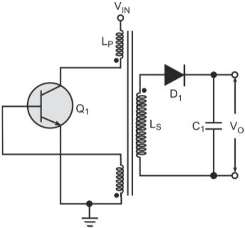
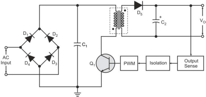
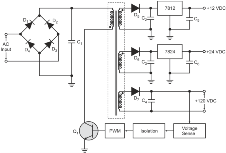
Figure below shows the basic schematic arrangement of an externally driven flyback converter.
Assume,
VIN = Input voltage in volts
VO = Output voltage in volts
PO = Output power to be delivered to load in watts
PIN = Power drawn from input source of power in watts
n = Expected conversion efficiency
tON = Conduction time in seconds
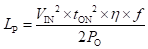
LP = Primary inductance in Henries
IP = Peak primary current in Amperes
IS = Peak secondary current in Amperes
NP = Primary turns
NS = Secondary turns
BMAX = Maximum flux density in the core in Weber/m2
ϕ = Magnetic flux in the core in Weber
Ac = Core cross-section in m2
W A = Window area in m2
f = Switching frequency
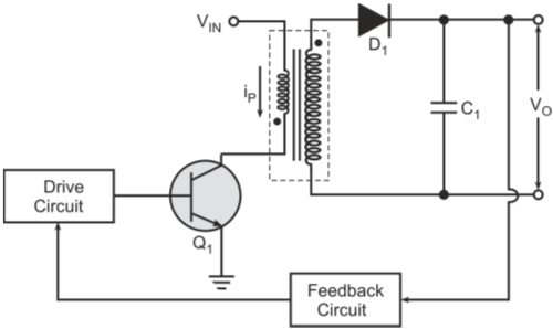
Externally driven flyback converter
Design of switching transformer
• The first step is to determine the size of the core in terms of the minimum area product required to deliver the desired amount of power to the load for the chosen values of operating frequency and maximum allowable temperature rise of the core.
• The area product is the product of winding window area and the cross-sectional area of the core.
• Designers can use these nomograms to choose suitable core for their application. Nomograms are curves that indicate the power-handling capability of different types of cores by a manufacturer as a function of operating frequency and given temperature rise. These nomograms are specific to the cores offered by the manufacturer. One such representative family of curves for toroidal ferrite cores is shown in Figure below.
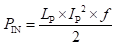
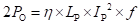
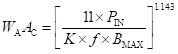
• The required area product can be computed from known values of input power, operating frequency and maximum permissible flux density as given by equation below.
Where,
WAAC is the area product in cm4
PIN is the power drawn from input source of power in W
f is the switching frequency in Hz
BMAX is the maximum flux density in the core in Weber/m2
K is the overall copper utilization factor. It is the product of three factors, namely, primary area factor (ratio of effective primary area to the available window winding area), winding packing factor (typically 0.35–0.4) and RMS current factor (ratio of effective DC input current to RMS value of primary current). K is typically in the range of 0.1 to 0.2.
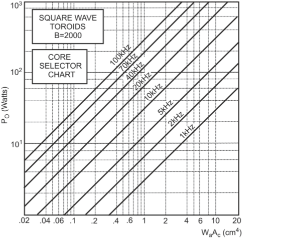
Power versus area product (WAAC) as function of switching frequency
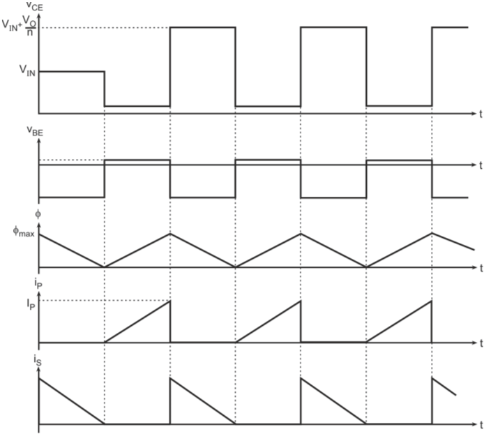
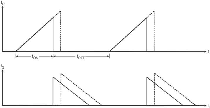
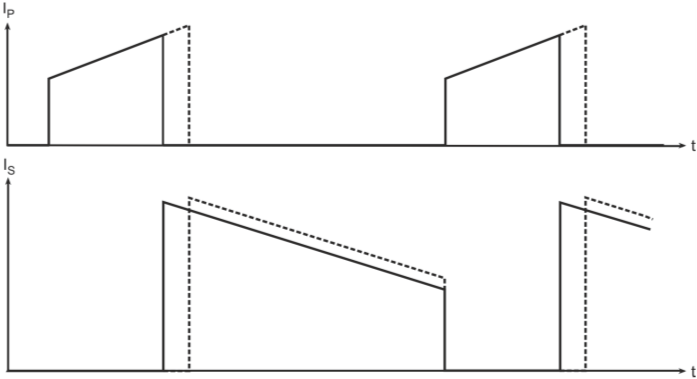
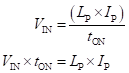
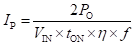
• When the switching transistor is switched on for a time period equal to tON, then the peak primary current IP can be computed from
• Also,
and
Therefore,
• On combining the above equations, we get
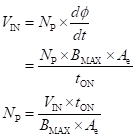
• The next step is to determine the number of primary turns that would not saturate the core. From first principles,
BMAX to be substituted in the above expression should be a little less than the BMAX rating of the chosen core material.
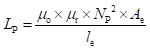
• The next step is to determine the size of air gap that would give a primary inductance of LP with NP number of primary turns. Primary inductance can also be computed from
Where,
µ0 is the permeability of free space = 4π x 10-7 H/m
µr is the initial relative permeability of the chosen core material
le the effective magnetic path length
The value of effective permeability µe that would make NP turns of the primary winding give LP Henries of primary inductance is calculated using the above equation.
• Having determined the value of µe, the size of the air gap can then be found from
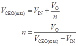
• The number of secondary turns can be determined from the known value of primary turns and the step-up ratio n.
• The step-up ratio is primarily decided by the VCEO(max) rating of the bipolar transistor or the VDS(max) rating of the MOSFET depending upon the switching transistor used in the circuit. In the case of bipolar transistor switch, during the turn-off time of the device, maximum voltage that appears across the collector–emitter terminals is given by VIN + VO/n, where n = NS/NP. Therefore,
This gives,
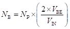
• The value of VCEO(max) to be substituted in the above equation should be less than the VCEO(max) rating given in the transistor’s data sheet. Drive circuit parameters can be determined from the required value of the base current IB
Primary and secondary wire sizes can be determined from calculated RMS values of primary and secondary currents.
Design of other blocks
• Diode D should be a fast recovery rectifier. A fast recovery rectifier ensures that the diode is fully reverse-biased and there is no leakage of power during the conduction time of the transistor.
• The peak inverse voltage (PIV) rating of the rectifier should be more than twice the desired output voltage.
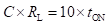
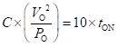
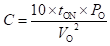
• Capacitor C should be such that time constant CRL provides the desired output ripple specification.
• CRL should be much larger than the turn-on time of the switching devices. It is chosen to be at least 10 times the turn-on time (tON). That is
This gives,