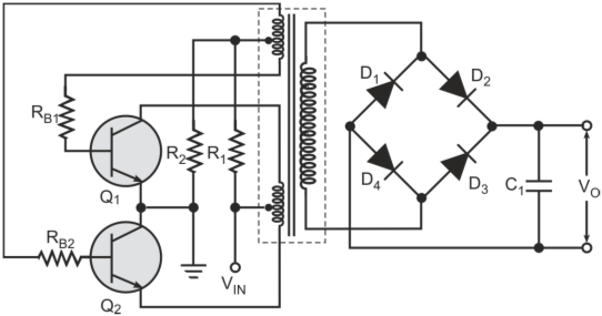
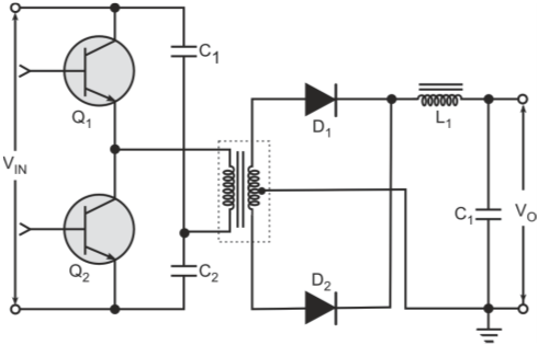
Figure below shows the configuration of the converter along with relevant diagrams. Step-by-step design procedure is outlined as follows.
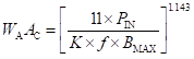
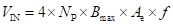
• First step is to determine the size of the core in terms of the minimum area product required to deliver the desired amount of power to the load for the chosen values of operating frequency and maximum allowable temperature rise of the core.
• The selection of the core size is done either with the help of nomograms provided by the manufacturer or by using the generalized expression given by
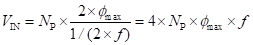
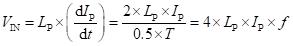
• From the first principles,
Where,
NP is the number of primary turns in the collector circuit of either of the two switching transistors = half of the primary turns.
• The magnetic flux varies from -Φ max to + Φ max or + Φmax to -Φ max when either of the two transistors is conducting. In both cases, change in magnetic flux equals 2 Φ max. That is
• Also, this change in flux occurs in a time period equal to half of the total time period. That is
Where,
T is the time period of switching waveform
T = 1/f, f being the switching frequency. Therefore,
Therefore,
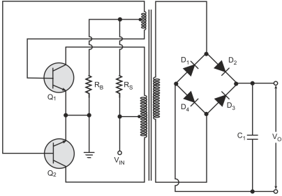
(a)
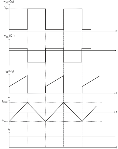
(b)
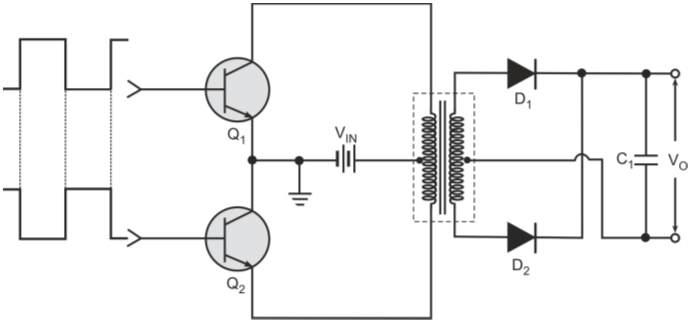
Self-oscillating push–pull converter: (a) circuit diagram; (b) waveforms
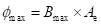
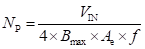
Now,
Where,
Bmax is the maximum flux density in the core and Ae the effective area of core cross-section.
• This gives
Therefore,
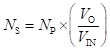
• Number of secondary turns NS can be computed from
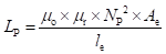
• From the known values of primary turns and core parameters, primary inductance can be determined from
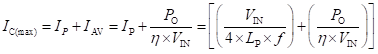
• The primary inductance then determines the peak value of primary current, which can be computed as follows.
Therefore,
• Maximum value of transistor’s collector current is then given by
The chosen transistors should be capable of handling this amount of collector current.
• Maximum value of collector-to-emitter voltage appearing across each of the transistors equals [2VIN + VBE (winding)]. VCEO(max) of the chosen transistor should be about 25–30% higher than this value.
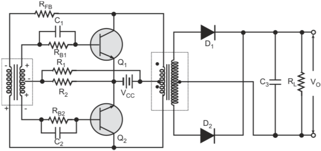
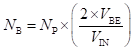
• NB can be determined in the same way as in the case of self-oscillating flyback converter. That is
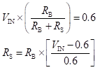
• RB should be such that it produces a voltage of 0.6 V at the center tap of the feedback winding. That is
• D1–D4 are rectifier diodes. These diodes should have the requisite PIV and forward current ratings.
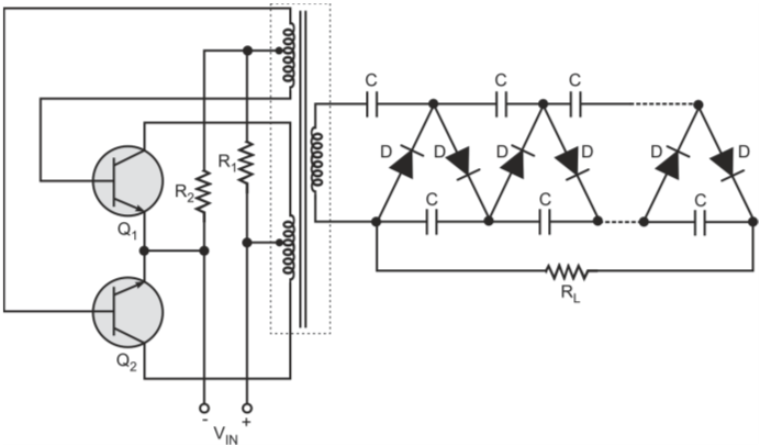
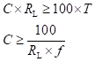
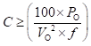
• Capacitor C is chosen to meet the specified output ripple requirement. Capacitor C is usually chosen to make CRL time constant much larger than (usually 100 times) the period T. That is
• Substituting
in the expression for C, we get