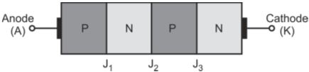
Figure below shows a PNPN diode represented as back-to-back connected NPN and PNP transistors. However, two transistors connected back-to-back do not make a PNPN diode.
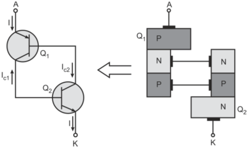
PNPN diode represented as back-to-back connected NPN and PNP transistors
Both the transistors are in active region because the collector junctions of both of them (i.e., J2) are reverse-biased and their emitter junctions (J1 of PNP transistor and J3 of NPN transistor) are forward-biased.
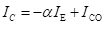
The collector current of a bipolar transistor in the active region is given by
Where,
IC is the collector current
α the short-circuit gain of CB configuration
ICO the reverse saturation current.
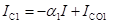
IE1 = Emitter current of Q1 = +I and IE2 = Emitter current of Q2 = -I
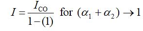
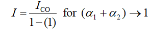
Also, the leakage current for Q1 (ICO1) is negative and for Q2 (ICO2) is positive. Let ICO be the total leakage current of the device. Therefore,
Hence
Now in the case of transistor Q1, substituting the sum of all currents entering the transistor equal to zero, we get
Substituting different values, we get
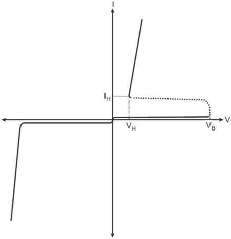
Here a1 and a2 are the forward current gains of the two transistors in common-base configuration. Their values are between 0 and 0.95 depending upon the currents flowing through them. When we are increasing the voltage, effectively we are doing nothing but increasing the value of a1 and a2 and when a1 + a2 reaches unity, there is a sudden increase in anode current as