Common-Emitter Biasing Circuits – part – I

  • Why is common-emitter configuration the most popular of the three transistor amplifier configurations?

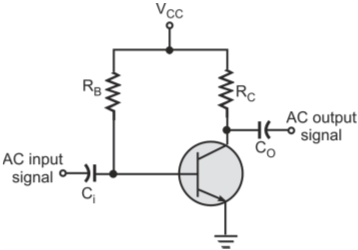
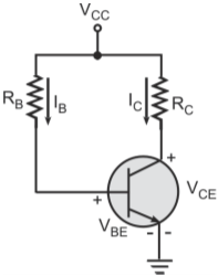
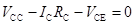
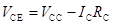
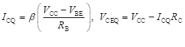
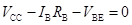
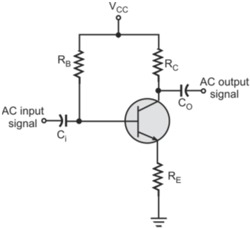
    Common-emitter configuration is the most popular of the three transistor amplifier configurations because it offers considerable current gain as well as voltage gain.

  • Name few common-emitter biasing circuits?

    Some of the commonly used common-emitter biasing circuits include the following

    • Fixed bias circuit
    • Emitter bias circuit
    • Voltage-divider bias with emitter bias circuit
    • Collector-to-base bias circuits

  • Draw the circuit diagram of fixed-bias circuit?

    Figure below shows the fixed-bias circuit. It is one of the simplest possible transistor-biasing circuits. The biasing components for this circuit include two resistors, base resistor (RB) and collector resistor (RC), and a supply voltage (VCC). Typical values of resistors RB and RC is of the order of few hundreds of kilo-ohms and few kilo-ohms respectively. Capacitors Ci and Co are referred to as the input and the output coupling capacitors, respectively. The base–emitter junction gets forward-biased through supply voltage (VCC) and RB. The collector–base junction is reverse-biased through supply voltage (VCC) and resistor RC.

    Fixed-bias circuit

  • Do DC analysis of a fixed-bias circuit?

    Figure below shows the DC equivalent of a fixed-bias circuit.

    DC equivalent of fixed-bias circuit

    Applying Kirchhoff’s voltage law to the base–emitter section, we get

    The value of base current (IB) therefore is

    As VBE << VCC, base current (IB) can be approximated as

    The collector current (IC) of the transistor is given as

    Where,
    β is the transistor current gain.

    Therefore,

    Applying Kirchhoff”s voltage law to the collector–emitter section we get

    Or

    Hence, the quiescent point for a fixed-bias circuit is given by

  • Perform the load-line analysis of a fixed-bias circuit?

    If we superimpose the straight line defined by Vcc-lB RB-VBE= 0 on the transistor output characteristics, we can determine the operating point of the circuit and also how the operating point changes with change in the value of circuit parameters. This is referred to as load-line analysis.

    To draw the load line, substitute IC = 0 in equation

    We get

    This point appears on the horizontal axis (0, VCC) of the output characteristics

    IC can be evaluated by substituting VCE = 0 in equation

    We get

    This point appears on the vertical axis (VCC/RC, 0) of the output characteristics.

    The load line is obtained by joining these two points as shown in Figure below. The operating point is established on the load line by determining the level of base current (IB). The point of intersection of the load line with the curve corresponding to the calculated value of IB gives the operating point as shown in the figure. The operating point shifts with the change in the value of circuit parameters.

    Load-line analysis of the fixed-bias circuit

  • How does the operating point change with change in base current for a fixed bias circuit?

    The operating point moves up the load line if the value of IB increases and moves down the load line when the value of IB decreases as shown in Figure below.

    Variation of operating point with base current

  • How does the operating point change with change in collector resistor for a fixed bias circuit, with all other parameters held as constant?

    With all other parameters held constant and the value of the collector resistor (RCis changed, then the load line shifts as shown in Figure below.

    Variation of operating point with collector resistor

  • How does the load line for a fixed-bias circuit vary with the supply voltage?

    The variation of the load line and the operating point due to change in the supply voltage (VCC) is illustrated in Figure below.

    Variation of operating point with supply voltage

  • List the advantages and disadvantages of a fixed-bias circuit?

    The advantage of a fixed-bias circuit is that it is the simplest possible biasing circuit requiring a very few components. However, it offers worst stability against variations in temperature or transistor gain (β) as compared to the other configurations. It is prone to thermal runaway and is very rarely used.

  • What is the emitter-bias configuration?

    Emitter-bias configuration (also referred to as self-bias circuit) is the same as that of fixed-bias circuit except that it has an emitter resistor (RE) between the transistor–emitter terminal and ground. Figure below shows the circuit diagram of an emitter-bias circuit.

    Emitter-bias configuration

  • What type of feedback is introduced by the addition of resistor RE in the emitter-bias configuration?

    The addition of the resistor RE introduces current-series negative feedback as a voltage proportional to the output current is fed-back into the input. This provides improved stabilization to the circuit.

  • Perform the DC analysis of an emitter-bias circuit?

    . Figure below shows the DC equivalent of the emitter-bias configuration.

    DC equivalent of the emitter–bias configuration

    Applying Kirchhoff’s voltage law to the base–emitter loop we get

    As IE = (β + 1)IB, the above equation can be simplified to give base current as given below

    As Voltage VBE is small as compared to VCC, it can therefore be neglected. Therefore,

    The value of the input resistance for the emitter-bias circuit is given by

    Applying Kirchhoff’s voltage law to the collector–emitter loop, we get

    Collector–emitter voltage (VCE) is therefore expressed as

    As the emitter current (IE) is approximately equal to the collector current (IC), therefore

    The voltage of the emitter terminal of the transistor (VE) is given by

    The Q-point for the emitter-bias circuit is given by

  • How does emitter-bias circuit offer better stability?

    The emitter-bias circuit offers stability against variations in collector current (due to change in temperature or change in the transistor gain (β)). When the collector current increases, the emitter voltage increases which in turn results in a decrease in the base–emitter potential. This further leads to a decrease in the value of base current and therefore, the collector current also decreases. This compensates for the initial increase in the value of collector current.

  • Do the Load-line Analysis of emitter-bias circuit?

    The load line for emitter-bias configuration is given by

    Substituting IC = 0 in above equation, we get

    This point appears on the horizontal axis (0, VCC) of the output characteristics.

    Substituting VCE = 0 in above equation, we obtain IC as

    This point appears on the vertical axis (VCC/(RC + RE), 0) of the output characteristics.

    The load line is obtained by joining these two points as shown in Figure below. The operating point is established on the load line by determining the level of IB.

    Load-line analysis of the emitter-bias circuit

  • What are the advantages and disadvantages of emitter-bias circuit?

    The emitter-bias circuit offers better stability as compared to the fixed-bias circuit. However, maximum stability is offered by the circuit when the ratio RB/RE is as small as possible. Thus, RE should have a large value or RB should have a small value.

    If the value of resistor RE is large, larger collector supply voltage (VCC) is required. In addition, increase in RE increases the negative feedback and hence the gain of the circuit is reduced. For small values of resistor RB, a separate base supply voltage is needed. This which adds to the circuit complexity.

Got a voltage spike of curiosity?

Send your doubts now!