Common-Emitter Biasing Circuits - part II

  • Which configuration offers better stability than emitter-bias configuration?

    Voltage-divider bias with emitter-bias configuration provides better stability against variations in temperature and transistor gain than the emitter-bias configuration. It is the most commonly used transistor-biasing configuration.

  • What is the Voltage-divider bias with Emitter-Bias Configuration?

    It is also referred to as the voltage-divider bias configuration. The input section comprises a voltage divider of resistors RB1 and RB2 across the supply voltage VCC. The output section is same as the emitter-bias configuration. Figure below shows the circuit.

    Voltage-divider bias with emitter-bias

  • Perform the DC analysis of voltage-divider bias with emitter-bias?

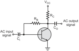
    The DC equivalent circuit of the voltage-divider bias with emitter-bias configuration is shown in the figure below.

    DC equivalent of voltage-divider bias with emitter-bias

    The circuit can be analyzed using two methods - accurate method and the approximate method. The accurate method is applicable to all circuits whereas the approximate method can be applied if under certain conditions.

    Accurate Method: It makes use of Thevenin’s equivalent model of the input section as shown in Figure below. RTH is the Thevenin’s equivalent resistance and is found by replacing the voltage source by a short circuit and calculating the resultant resistance of the circuit. RTH is given by

    VTH is the open-circuit Thevenin’s voltage and is equal to the voltage drop across the resistor RB2.

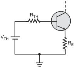
    Thevenin’s equivalent of the input section of voltage-divider bias configuration

    Figure below shows the complete circuit using Thevenin’s equivalent model.

    Thevenin’s equivalent of voltage-divider bias configuration

    Applying Kirchhoff’s voltage law to the base–emitter loop, we get

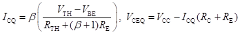
    Substituting IE = (β + 1)IB, we get the expression for IB as

    If VBE << VTH, then

    Collector–emitter voltage (VCE) can be determined by applying Kirchhoff’s voltage law to the collector–emitter loop,

    As IC ≌ IE,

    The operating point is given by

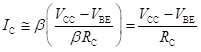
    Approximate Method: The equivalent resistance between the base terminal and the ground and is referred to as the input resistance. Its value is given by

    If the value of resistance Ri is much larger than the resistance RB2, then base current IB is assumed to be zero and resistors RB1 and RB2 can be considered as series elements.

    Voltage at the base terminal (VB) is given by

    The emitter voltage (VE) is expressed as

    Emitter current (IE) is given by

    As collector current (IC) and emitter current (IE) are approximately equal, the value of IC is

    The collector–emitter voltage (VCE) is given by

    Approximate method can be applied if the value of the input resistance Ri is equal to greater than 10 times the resistance RB2. That is

  • Perform the load-line analysis of voltage-divider bias with emitter-bias?

    The output circuit of the voltage-divider bias configuration is the same as that of the emitter-bias configuration. This results in the same load line for the two configurations. Load-line analysis can be carried on similar lines as to that for emitter-bias configuration.

  • Negative feedback in voltage-divider bias configuration results in reduction of AC gain of the circuit. How can this problem be solved?

    The problem of reduction in AC gain can be solved by using a capacitor CE in parallel with resistor RE (as shown in figure below). The capacitor does not affect the DC analysis as it acts as an open circuit for DC voltages. For AC voltages, it tends to be short circuit thus removing the problem of AC negative feedback.

    Voltage-divider bias configuration with emitter capacitor

  • Draw the circuit for collector-to-base bias configuration?

    Figure below shows the circuit for collector-to-base bias configuration (also referred to as feedback-bias). In this configuration, the base-bias voltage is obtained from the collector of the transistor instead of the collector supply voltage (VCC). It offers good stability of the operating point against variations in temperature and transistor gain (β) due to negative feedback.

    Collector-to-base bias configuration

  • Which type of feedback is present in collector-to-base bias configuration?

    The configuration has voltage-shunt feedback as the output voltage is fed-back in shunt to the input through base resistor (RB).

  • Perform the DC analysis of collector-to-base bias circuit.

    Figure below shows the DC equivalent of the collector-to-base bias circuit. The current in the resistor RC through supply voltage VCC is split into two parts at the collector junction: one part flowing into the collector terminal (IC) and the other part flowing through the base resistor (RB). The current in resistor RB is equal to the base current (IB). Therefore, the current through resistor RC is the sum of the base current (IB) and the collector current (IC).

    DC equivalent of collector-to-base bias configuration

    Applying Kirchhoff’s voltage law to the base–emitter loop, we obtain

    Substituting IC = βIB, in the above equation we get

    The value of collector current (IC) is given by IC = βIB. Therefore

    If the value of (β+1)RC >> RB, then the term (RB + (β+1)RC) can be approximated as βRC and in this case the value of collector current IC is

    Applying Kirchhoff’s voltage law to the collector–emitter loop, we get

    Ignoring base current (IB) as IB << IC, we get

    The value of the operating point for collector-to-base bias configuration is given by

  • Perform the Load-line Analysis for collector-to-base bias configuration?

    The load-line analysis for collector-to-base bias can be done on similar lines to that of emitter-bias configuration.

  • What are the advantages offered by collector-to-base bias circuit?

    The collector-to-base bias circuit provides stability to the operating point against variations in temperature and transistor gain (β).

  • What are the disadvantages offered by collector-to-base bias circuit? How can these disadvantages be countered?

    The main disadvantage offered by collector-to-base bias circuit is that due to negative feedback, the AC voltage gain of the amplifier is reduced. This problem is partially solved by splitting the resistor RB into two parts and by connecting a capacitor CB as shown in figure below.

    For AC signal, capacitor CB acts as a short circuit and the effective base resistance RB is reduced to half. This reduces the AC negative feedback and increases the AC voltage gain offered by the circuit.

    Collector-to-base bias with capacitor to reduce AC negative feedback

    Also, the base resistor (RB) in collector-to-base bias has a small value and therefore the base current changes more rapidly with temperature. Hence, the advantage of better stability factor offered by collector-to-base bias circuit is offset by the larger variation in the base current.

Got a voltage spike of curiosity?

Send your doubts now!