Common Base Biasing Circuits

  • Draw the circuit diagram of common-base configuration?

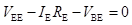
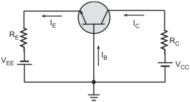
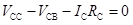
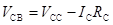
    Figure below shows the circuit diagram of common-base configuration. Here, the input is applied to the emitter terminal and the output is taken from the collector terminal. The base terminal is common to both the input and the output sections.

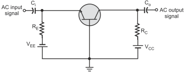
    Common-base configuration

  • Perform the DC analysis of common-base configuration?

    Figure below shows the DC equivalent circuit of common-base configuration. Applying Kirchhoff’s voltage law to the input section (emitter–base loop), we get

    Therefore, the emitter current (IE) is equal to

    DC equivalent of common-base circuit

    Applying Kirchhoff’s voltage law to the output section (collector–emitter loop), we get

    Therefore,

    The operating point for the common-base configuration is given by

  • Perform the load-line analysis for common-base configuration?

    The load line is drawn using the output equation given by

    Substituting IC = 0, we get

    Substituting VCB = 0, we get

    Joining the two points we can draw the DC load line on the output characteristics as shown in figure below. The operating point (ICQ, VCBQ) is determined by the point of intersection of the load line with the characteristic curves at the value of emitter current (IE).

    Load-line analysis of common-base configuration

Got a voltage spike of curiosity?

Send your doubts now!