Transistor Switch

  • Explain the operation of transistor as a switch?

    Transistors are used as switching devices in computers and other control applications. Figure below shows the use of a transistor as an inverting switch with the input and the output waveforms. When a logic-LOW input is applied, the transistor is in the cut-off region and the output is at logic-HIGH and acts as an open switch. It is in the saturation region for a logic-HIGH input, the output is at logic-LOW and acts as a closed switch.
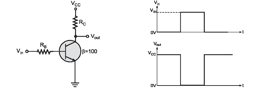
    Transistor switch circuit with input and output waveforms

    Logic-HIGH Input Condition: Transistor should be heavily saturated for a logic-HIGH input signal. The saturation collector current (IC(sat)) is given by the equation

    The level of base current (IB) in the active region just before the saturation region can be approximated by

    The base current (IB(max)) is kept to be 20–25% more than the value of IB(sat). This ensures ensure that the transistor is in deep saturation. Therefore, the ratio of the collector current to the base current when the logic-HIGH input is applied is less than the transistor current gain ( Β). The minimum value of input voltage (VIH) required to drive the transistor into deep saturation is given by

    The resistance between the emitter and the collector terminals when the transistor is in saturation is given by

    The resistance offered by the transistor switch when in saturation is equal to Rsat. The value of Rsat is in the range of few ohms to few tens of ohms. Logic-LOW Input Condition: For input voltage equal to zero, the collector current (IC) is equal to the leakage current (ICO). This current is negligible and hence the collector voltage is at the logic-HIGH level. Also, the collector–emitter resistance is very high in the range of several hundreds of kilo-ohms to few mega-ohms. The circuit thus acts as an open circuit.
  • Explain the switching delays of a transistor when it operates as a switch?

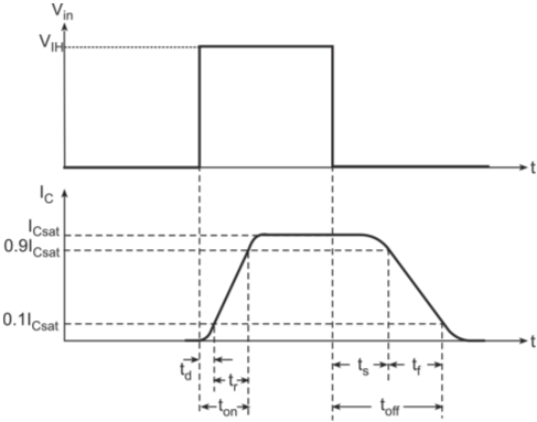
    Refer to figure below. It shows the response of a transistor switch when an input pulse is applied to it.

    Transistor switching times

    When the input voltage is 0 V, the transistor is in the cut-off region and is in the saturation region when the input voltage is at the voltage level VIH. When the input voltage changes from 0 V to VIH, the transistor does not immediately respond to the input signal. There is a time delay before the collector current reaches its saturation value and it comprises of the following two components.

    • Delay time: The time delay between the time the input pulse is applied to the time the collector current rises to 10% of the final value is called the delay time (td). Delay time (td) is contributed by three factors
    1. Time required to charge the emitter-junction capacitance so that the transistor is brought from the cut-off to the active region
    2. Time required to move the carriers from the base junction to the collector junction
    3. Time required by the collector current to rise to 10% of its final value
    • Rise time: The time required for the collector current to rise from 10% to 90% of the final value is called the rise time (tr). Rise time (tr) is due to the time taken by the collector current to traverse the active region.

    The total time (td + tr) is known as the turn-ON time (ton) of the transistor. When the input signal changes from HIGH to LOW, again there is a delay before collector current reduces to zero. This time delay again comprises of two components.
    • Storage time: The time interval between the input pulse transition to the time when the collector current drops to 90% of its value at saturation is called the storage time (ts). Storage time delay is because the transistor in saturation has a saturation charge of excess minority carriers stored in the base region and the transistor cannot respond until this excess charge has been removed.
    • Fall time (tf): It is the time required by the collector current to fall from 90% to 10% of the saturation level. Fall time is caused due to the time required by the collector current to traverse the active region.
    Turn-OFF time (toff) is defined as the sum of the storage time (ts) and the fall time (tf).

  • How can the storage time of a transistor be reduced?

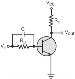
    Refer to figure below.

    Fast switching transistor circuit

    Adding a capacitor (C) across the base resistor (RB) reduces the storage time. The capacitor acts as a short circuit when switching occurs and an impulse current will flow out of the base at the negative transition of the input pulse.

Got a voltage spike of curiosity?

Send your doubts now!