The circuit functions as follows. Refer to the timing diagram in the figure below wherever required.
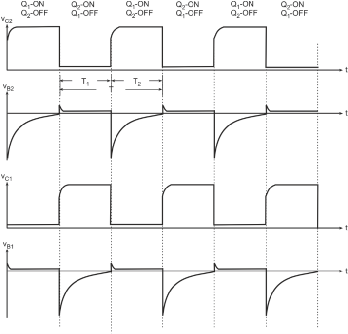
Timing waveforms of astable multivibrator
• When power is applied, one transistor will conduct more than the other because of some circuit imbalances. Let us assume that transistor Q1 conducts more than transistor Q2.
• The regenerative action will force transistor Q1 to saturation and transistor Q2 to cut-off. Capacitor C2 will charge rapidly to VCC through resistor RC2 and the base-emitter junction of transistor Q1.
• This results in momentary increase in the base voltage of transistor Q1. Capacitor C1 had previously charged through resistor RC1 upto VCC when transistor Q2 was conducting. Now when Q1 is conducting, C1 discharges through R1 and Q1.
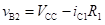
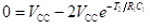
The base voltage of transistor Q2 during discharge of capacitor C1 is given by
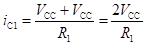
Since, the capacitor charges to approximately VCC, the initial value of current (iC1) is
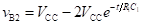
The current decays exponentially with a time constant of R1C1. Therefore, the voltage vB2 is given by
• The initial pulse of discharge current from C1 through R1 results in a negative pulse at the base of transistor Q2 as shown in figure below.
• This turns transistor Q2 OFF and the output goes to HIGH state. Transistor Q1 keeps conducting from VCC through resistor R2.
• The OFF-time of transistor Q2 depends upon the time constant R1C1. When the base voltage of the transistor reaches the base-switching voltage, transistor Q2 is no longer in cut-off and starts to conduct allowing capacitor C1 to be recharged rapidly through resistor RC1.
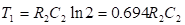
The base-switching voltage for silicon transistors is 0.5 V and that for germanium transistors is 0.2 V, which is very small as compared to the VCC voltage. Therefore, it can be assumed that the transistor will switch when vB2 = 0 V. The time required to switch ON transistor Q2, that is, the OFF time of the transistor Q2 (T2) is given by
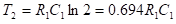
T2 is also the ON time of transistor Q1.
• This results in momentary increase in positive voltage at the base of the transistor Q2 leading to its fast turning ON. Therefore, the output goes to the LOW state.
• Now capacitor C2 discharges through transistor Q2 and resistor R2. The initial pulse of discharge current from C2 through R2 makes the base of transistor Q1 very negative. This turns OFF Q1.
• Q1 is held in the OFF state depending upon the time constant R2C2 after which Q1 begins to conduct.
ON time (T1) of transistor Q2 which is equal to the OFF time of transistor Q1 is given by
• This process continues and due to both the couplings (Q1-collector to Q2-base and Q2-collector to Q1-base) being capacitive, neither of the states is stable.
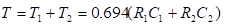
The total time period of the wave is T which is given by
•The rounding off in the rising edge of VC1 is because of the voltage drop across resistor RC1 while capacitor C1 is recharging. Similarly the rounding off in the rising edge of VC2 is because of the voltage drop across resistor RC2 while capacitor C2 is recharging.