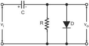
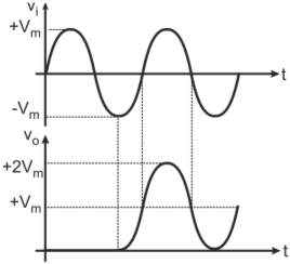
Figure below shows the input and the output waveforms for the negative clamper circuit of Q4 when the input signal applied is a sinusoidal signal.
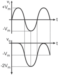
Input and output waveforms of a negative clamper circuitInput and output waveforms of a negative clamper circuit
The circuit functions as follows.
• As the input vi rises towards the positive peak Vm from zero in the first quarter of the cycle, capacitor (C) charges to Vm through the forward-biased diode.
• The overall charging resistance is sum of source resistance (Rs) (not shown in the figure) and the parallel combination of R and diode’s forward resistance (Rf). If R is much larger than Rf then the capacitor C charges with a time constant of [(Rs + Rf) C].
• C should be such that it charges to Vm in a time which in no case is greater than one-fourth of the time period of the input waveform. The total charging time may be considered to be equal to five times the time constant.
• When the input starts decreasing, the diode becomes reverse-biased. The capacitor now tends to discharge through resistor R.
• If the time constant (RC) is much larger than the time period of the input waveform, the discharge of the capacitor is negligible. Therefore, the voltage across the capacitor remains constant at the maximum value of the input signal.
• Output at any instant of time is then equal to algebraic sum of input voltage and voltage across the capacitor. Thus, all positive peaks (Vm) are clamped to zero and all negative peaks (–Vm) go to –2Vm. Therefore, the clamping circuit does not alter the wave shape, it only changes the DC level.
• When the peak value of the input signal increases, the capacitor charges through the forward-biased diode again to the new larger value and when the peak value of the input signal decreases, it discharges through R to the new lower value.